Terahertz scattering-type scanning near-field optical microscopy (THz s-SNOM) is a nano-imaging technique that breaks through the optical diffraction limit, and is particularly suited to the THz band (wavelength around 300 μm). Conventional optical microscopes cannot resolve structures much smaller than the wavelength, whereas s-SNOM exploits the field-enhancement effect at a metal probe tip to achieve nanoscale spatial resolution.
Previous research has mostly focused on imaging surface structures, with relatively little work on imaging metal structures buried deep beneath dielectric layers — especially when the covering layer is much thicker than the probe tip radius. The literature discussed in this article successfully achieved high-contrast imaging of metal lines buried beneath a silicon oxide (SiO₂) layer (covering layer thickness ≈ 200 nm, probe radius ≈ 40 nm, i.e., a thickness about 5 times the probe radius), which is of great significance for non-contact failure analysis in the semiconductor industry.
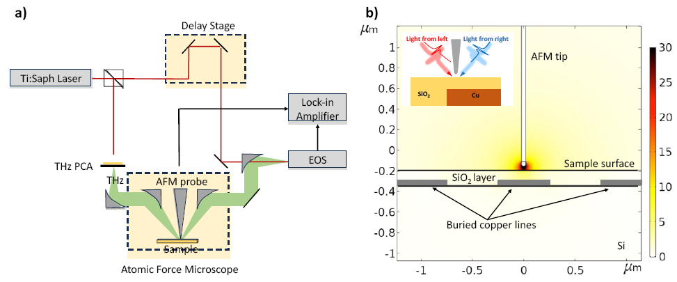
Figure 1(a) shows the experimental setup, and Figure 1(b) depicts the simulation model under equivalent experimental conditions. The experiment used a platinum-iridium (PtIr) conical probe with a tip radius of 40 nm and a tip length of 80 μm. The AFM tip oscillated vertically on the sample surface with an amplitude of 250 nm and a vibration frequency of 16 kHz. This amplitude is relatively large compared to typical cases; the larger amplitude improves the signal from subsurface structures. The probe tip was illuminated by broadband THz pulses generated by a photoconductive antenna located outside the AFM. The radiation scattered from the tip was measured using free-space electro-optic sampling, and the desired near-field signal was obtained through lock-in demodulation.
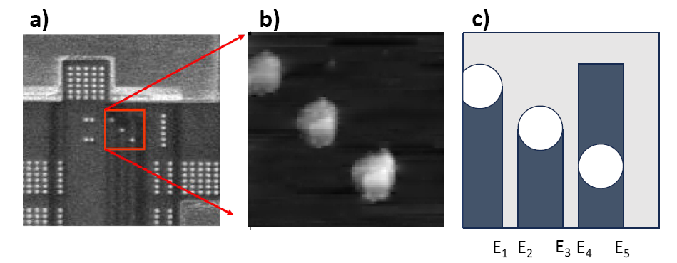
The experimental sample was a silicon-based chip structure, with the structural cross-section shown in Figure 2. The region of interest in the study has relatively simple morphological features, making it suitable as a test platform for analysis. This region contains three copper interconnect lines buried beneath a dielectric layer, corresponding to the simulated region in Figure 1(b). Specifically, these copper lines were deposited on the underlying planarized silicon substrate, with a designed width of 0.75 μm and a spacing of 0.45 μm between adjacent lines. In the scanning electron microscope (SEM) image, the vertical traces of the copper lines can be faintly discerned (see Figure 2(a)); however, in the atomic force microscope (AFM) topography map, their morphological features are completely invisible. After completing the terahertz (THz) imaging measurements, a focused ion beam (FIB) system was further used to precisely characterize the thickness of the SiO₂ dielectric layer in the target region, which was measured to be 209 ± 20 nm.
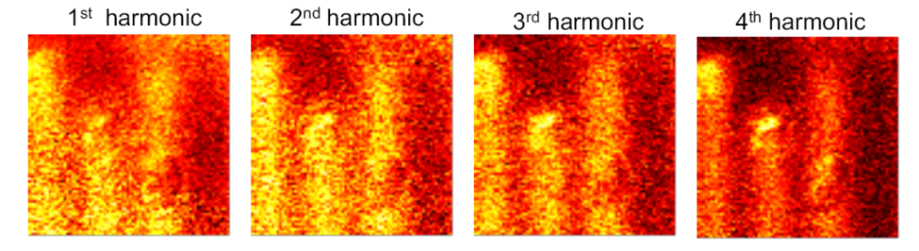
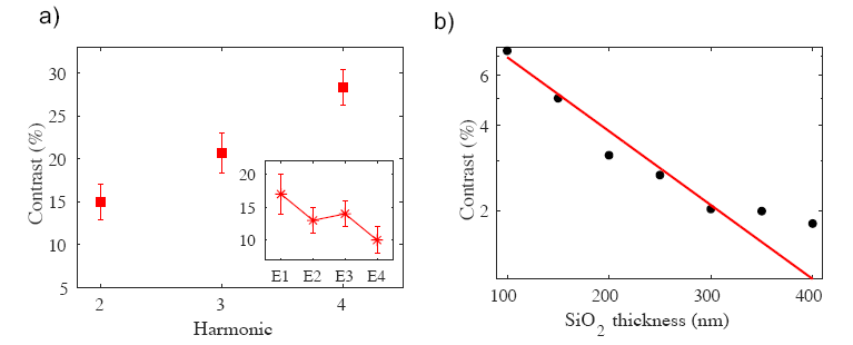
Figure 3 shows the 1st- to 4th-order optical signal imaging of the test sample. Figure 3 demonstrates that the imaging capability of THz s-SNOM for deeply buried metal lines depends significantly on the harmonic order of signal demodulation. As the demodulation order increases, the contrast improves — for example, the contrast of the 4th harmonic is nearly twice that of the 2nd harmonic (Figure 4a) — because higher harmonics more effectively suppress far-field background noise.
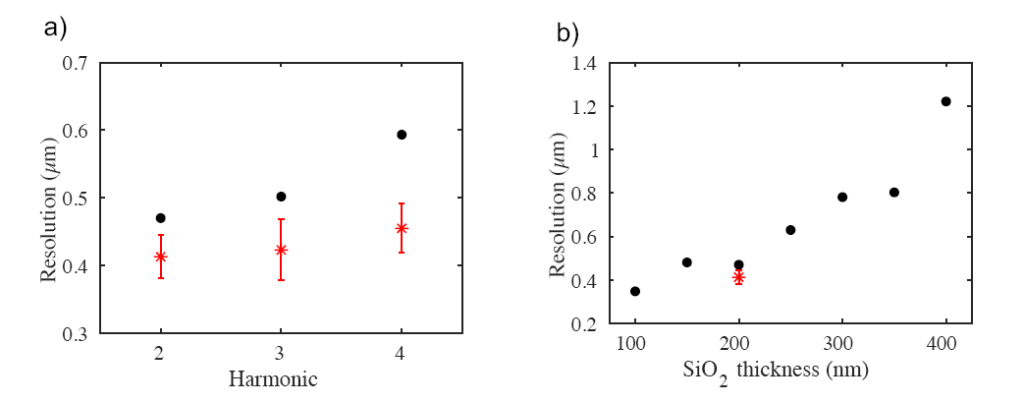
However, the authors found in both experiment and simulation that spatial resolution is better for lower harmonics (Figure 5a), contrary to initial expectations. At higher harmonics, the source of the scattered signal becomes more localized to the AFM tip, which improves the lateral spatial resolution of structures exposed at the surface. For buried structures, however, the increased localization poses a challenge. As the distance between the tip and the buried structure grows, the localized nature of higher harmonics also means increased vertical confinement of the signal, resulting in weaker signals from structures buried beneath the surface. Therefore, while higher harmonics improve the overall contrast and resolution of surface features, they simultaneously reduce the signal strength of buried features, reflecting a resolution trade-off between imaging buried structures and exposed structures.
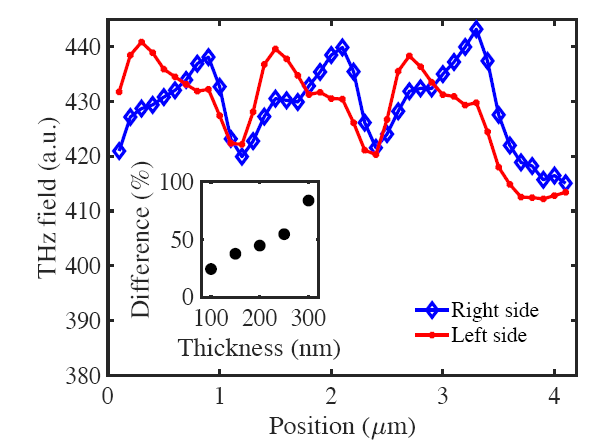
In addition, both simulation and experiment found a directional dependence of the signal at the metal line edges, as shown in Figure 6. On the side of a metal line facing away from the incident light, the signal intensity exhibits an overshoot of 10–15% (red and blue curves in Figure 6). For example, when THz waves are incident from the right side, the contrast of the left edges (E2, E4) is lower than that of the right edges (E1, E3) (inset of Figure 4a). This asymmetry originates from the shadowing effect of the probe — after obliquely incident light is blocked by the probe, the scattered signal on the shadowed side becomes stronger. Simulations further show that when the covering layer thickness increases to 300 nm, the overshoot becomes the primary basis for resolving structures.
In summary, the literature cited in this article points out that the depth imaging capability demonstrated in this study significantly exceeds previously reported results, indicating that THz s-SNOM may be a valuable tool for investigating buried metallization layers, which has positive significance for advancing THz imaging development.
References
Ma P, Kölbel J, Ying JF, Lin JH, Pizzuto A, Mittleman DM. Terahertz near-field imaging of buried structures. Opt Express. 2024 Oct 21;32(22):39785-39792. doi: 10.1364/OE.532478. PMID: 39573788.
-END-
Text|Yu Shuchao
Layout|Xiang Shaolian