Author: Zhang Tianyu
Introduction: Recently, Edmund J. R. Kelleher and Peter U. Jepsen of the Technical University of Denmark (DTU), together with their collaborators, used scattering-type scanning near-field optical microscopy (s-SNOM) combined with terahertz time-domain spectroscopy (THz-TDS) to achieve nanoscale quantitative imaging of the dielectric permittivity of MoS₂ nanoribbons (spatial resolution ≈ 30 nm).
By developing an inversion algorithm based on the finite dipole model (FDM), they extracted, for the first time, the featureless dielectric spectrum of MoS₂ nanoribbons in the 0.6–1.6 THz band, and found that: the mean real part of the permittivity in the nanoribbon core region is Re{ε} = 5.43 (consistent with reported bulk material values in the literature); the real part of the permittivity decreases by ≈ 10% in the edge regions due to strain; and four types of dielectrically heterogeneous regions were identified through cluster analysis, revealing nanoscale dielectric disorder.
This research was published in the internationally renowned academic journal Nanophotonics under the title "Dielectric Permittivity Extraction of MoS₂ Nanoribbons Using THz Nanoscopy". The corresponding author is Edmund J. R. Kelleher, and the first author is Henrik B. Lassen.
Research background: Transition metal dichalcogenides (TMDs) such as molybdenum disulfide (MoS₂) have important application potential in nanoscale optoelectronic devices due to their unique layered structures and tunable optoelectronic properties. As one-dimensional confined structures, the dielectric permittivity of MoS₂ nanoribbons directly affects carrier mobility, optical response, and device performance.
However, conventional characterization techniques have significant limitations: far-field terahertz time-domain spectroscopy (THz-TDS) is limited by the diffraction limit, with a spatial resolution of only about one hundred micrometers, unable to resolve nanoscale heterogeneity; Raman and photoluminescence spectroscopy can probe crystal structure but cannot directly obtain the dielectric function; electrostatic force microscopy (EFM) is only applicable to static field measurements and lacks frequency-band coverage.
Moreover, the influence of dielectric disorder in nanomaterials (such as edge strain and defect distribution) on device performance has not yet been quantified. Current techniques struggle to achieve dielectric imaging with nanoscale spatial resolution (<50 nm) in the terahertz band (0.1–10 THz), hindering a deeper understanding of the intrinsic properties of low-dimensional materials. Therefore, developing a method that combines high spatial resolution with broadband detection capability has become a key challenge in revealing the dielectric behavior of MoS₂ nanoribbons.
Research content and results:
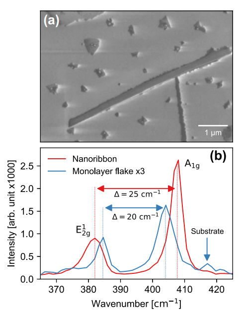
SEM images (Fig. 1a) show the macroscopic morphology of the MoS₂ nanoribbons (length ≈ 10 μm, width <0.5 μm), with dispersed monolayer/multilayer crystals observed nearby. Raman spectroscopy (Fig. 1b) shows that the core region of the nanoribbon has bulk-like characteristics (E₁₂g and A₁g peak separation of 25 cm⁻¹), while AFM analysis ruled out the influence of residual strain, indicating a structurally stable core region.
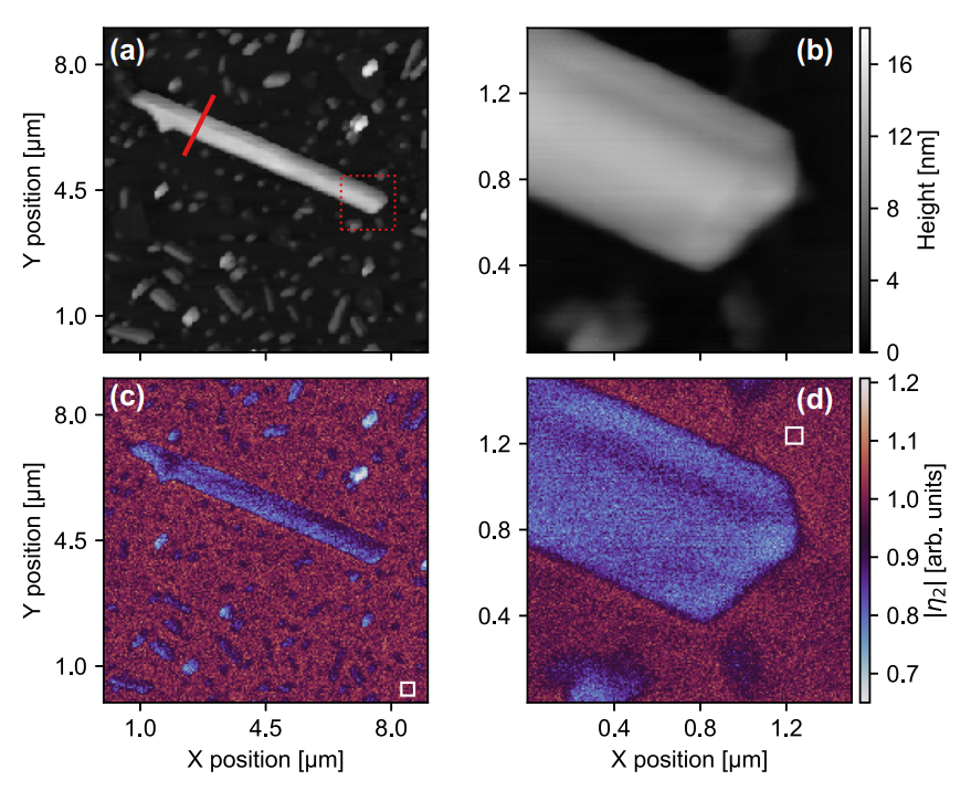
AFM images (Fig. 2a-b) precisely measured the nanoribbon thickness as 10–15 nm (>15 layers), but did not resolve the monolayer edge structures visible in SEM. White-light near-field imaging (Fig. 2c-d) revealed, for the first time, the spatial distribution of dielectric contrast in the nanoribbon: the scattering signal intensity of the nanoribbon is only 50% of that of the sapphire substrate (η₂≈0.5), and abrupt changes appear at the edge regions (resolution ≈ 50 nm), demonstrating a coupling effect between morphology and dielectric properties.
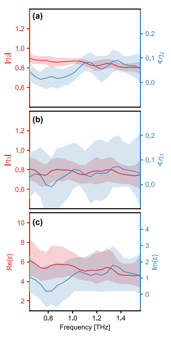
Terahertz nano-line scans (Fig. 3a-b) show that the dielectric response of the nanoribbon core region exhibits no characteristic fluctuations in the 0.6–1.6 THz band (real part stable at 0.5, imaginary part close to zero). The complex permittivity spectrum was extracted through finite dipole model (FDM) inversion (Fig. 3c), with a mean real part Re{ε} = 5.43 (fluctuation <±0.1), in close agreement with the bulk static permittivity values reported in the literature, confirming an extremely low carrier concentration in the nanoribbon core region.
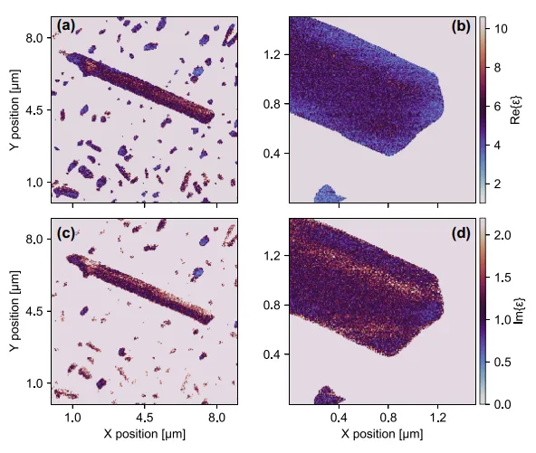
A dielectric spatial distribution map was generated based on white-light imaging data (Fig. 4a-d), showing a uniform distribution of the real part of the permittivity in the core region (ε'≈5.4, standard deviation <0.08), while ε' drops significantly to ≈4.9 (a 10% decrease) in the edge regions. The imaginary part ε'' approaches zero across the entire region, highlighting the low-loss characteristics of the material. This result represents the first quantitative dielectric imaging at 30 nm resolution.
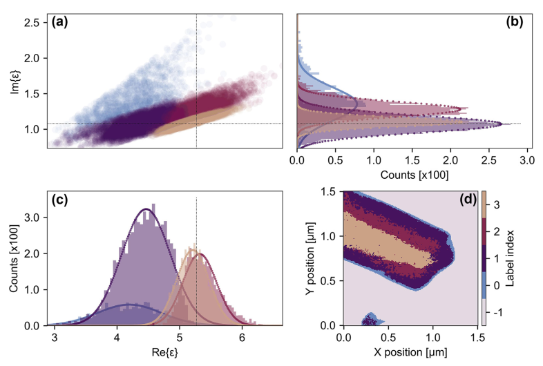
A Bayesian Gaussian mixture model (Fig. 5a) identified four dielectric clusters:
1. Edge regions (Cluster 0): ε'≈4.9; AFM curvature analysis indicates that high strain leads to the reduced permittivity;
2. Core regions (Clusters 2 & 3): ε'≈5.4, with concentrated distribution (σ≈0.08), reflecting uniform dielectric properties;
3. Transition regions (Cluster 1): ε'≈5.1. Spatial mapping (Fig. 5d) confirms that the 10% permittivity decrease at the edges mainly originates from local strain rather than intrinsic defects.
Future prospects: Based on this breakthrough research on the dielectric behavior of MoS₂ nanoribbons using terahertz nanoscopy, future work can be deepened in the following directions:
1. Technical optimization and extension: develop anisotropic dielectric tensor separation algorithms, combined with probe polarization control techniques, to achieve independent resolution of in-plane/out-of-plane dielectric components of materials (e.g., using the mid-infrared band to probe phonon mode responses). Improve spatial resolution by optimizing tip fabrication (e.g., single-atom tips) and signal processing algorithms (e.g., deep learning denoising), enabling dielectric imaging of single-atom defects.
2. Generalization to more material systems: extend the method to other two-dimensional materials (such as WS₂, WSe₂) and one-dimensional heterostructures (such as MoS₂/graphene lateral junctions), establishing a universal correlation model between dielectric properties and dimensionality effects. Explore the dynamic tuning of permittivity through strain engineering, quantifying the strain-dielectric coupling coefficient with in-situ stretching devices (target accuracy ±0.1).
3. Device application driven: reveal the influence of dielectric disorder (such as edge strain and defect clusters) on the mobility of nanoribbon transistors (with the goal of establishing a quantitative Δε/Δμ relationship), guiding high-performance device design. Develop dielectric-map-assisted defect repair strategies (such as laser annealing and chemical passivation) to suppress local dielectric fluctuations to <5%.
4. Interdisciplinary integration: combine multimodal characterization (such as scanning microwave impedance microscopy and ultrafast spectroscopy) to build a full-parameter model of dielectric-carrier-lattice dynamics, advancing the application of low-dimensional materials in quantum light sources and sensing chips.
Paper information: Lassen, Henrik B., Carstensen, William V., Miakota, Denys I., Ghimire, Ganesh, Canulescu, Stela, Jepsen, Peter U. and Kelleher, Edmund J. R.
"Dielectric permittivity extraction of MoS2 nanoribbons using THz nanoscopy"
Nanophotonics, vol. 14, no. 10, 2025, pp. 1673-1682.