Shenzhen University: Visible-Light Near-Field Upgrade Delivery and Testing
In 2024, our company successfully delivered a three-wavelength visible/near-infrared near-field optical microscopy imaging system to Shenzhen University. The system is equipped with an original Neaspec atomic force microscope, visible/near-infrared continuous-wave light sources and a precision near-field coupling optical path, enabling nano-resolution near-field optical imaging at 532 nm, 785 nm and 1064 nm.
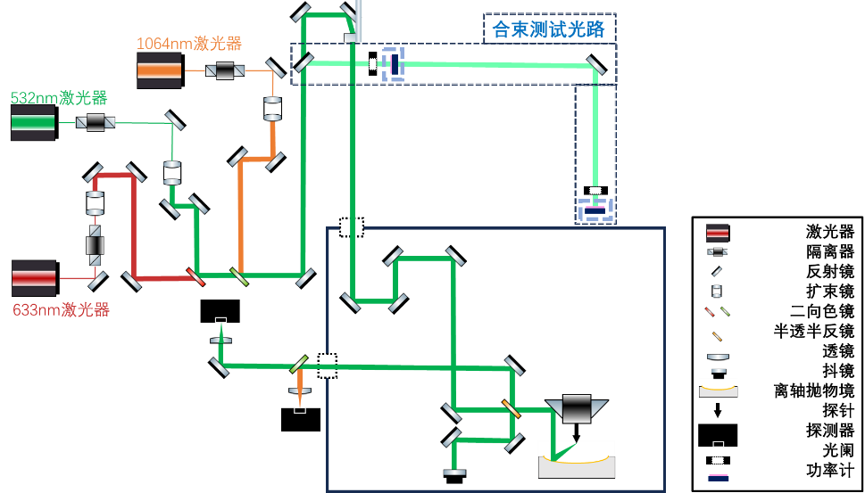
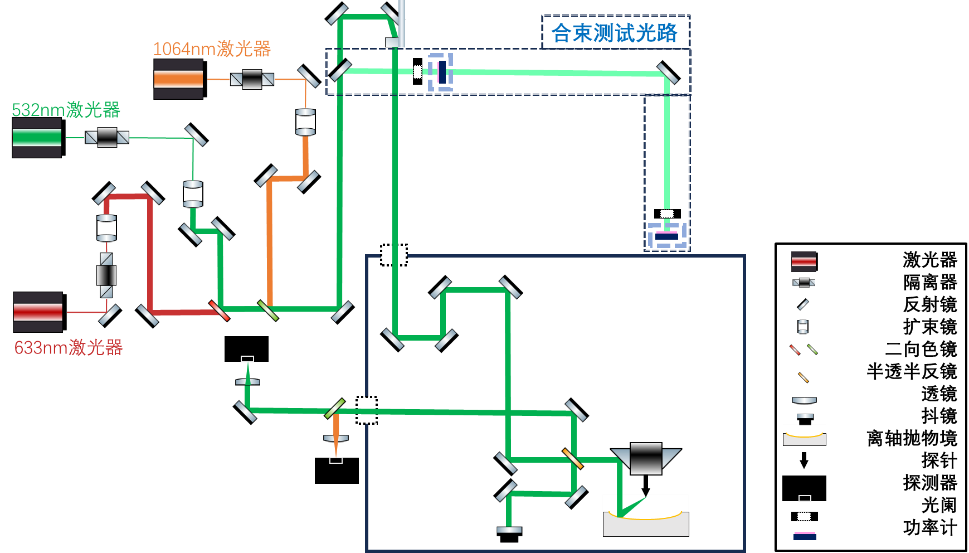
Optical path schematic of the visible-light near-field optical imaging system
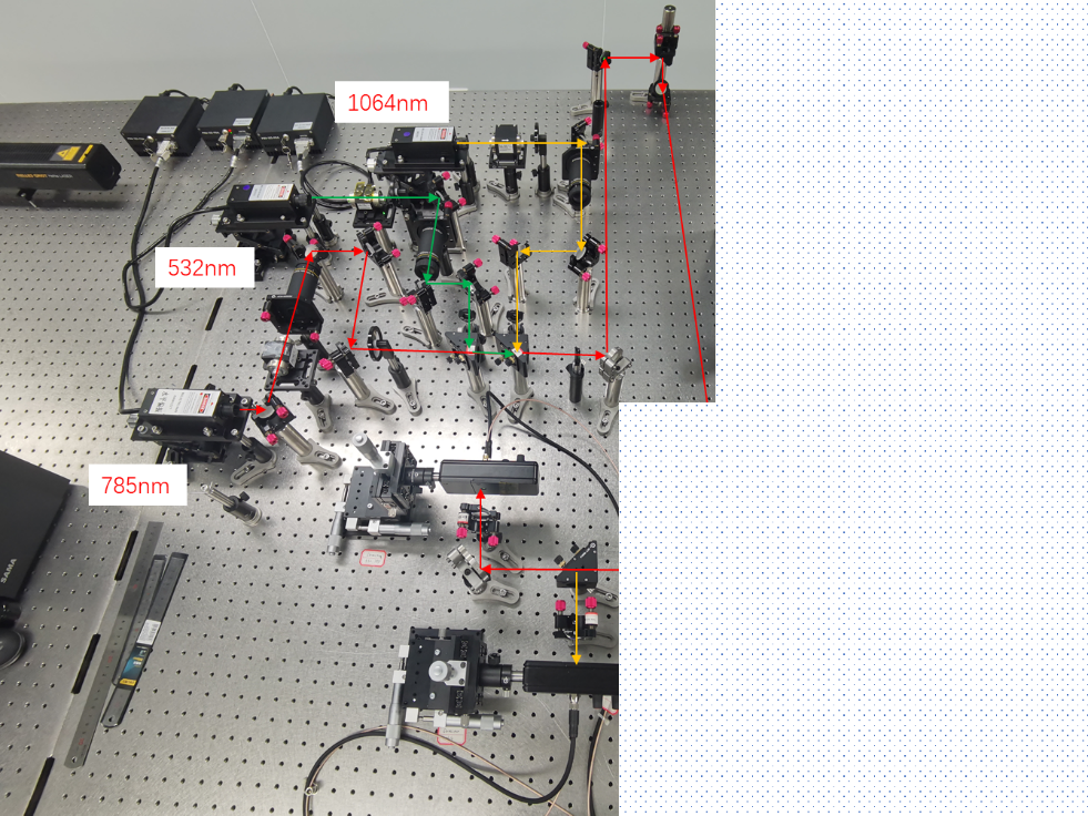
Physical optical path of the visible-light near-field optical imaging system
System Overview
In this system, the beams of the three wavelengths are expanded, collimated and combined into a single optical path via two dichroic mirrors, and then overlapped with the original neaspec infrared near-field optical path. The upgraded visible-light near-field system still uses a pseudo-heterodyne interferometric optical path: after phase modulation by a dithering mirror, the reference light enters the photodetector together with the near-field signal scattered by the probe and the background signal reflected by the atomic force cantilever. If the probe tapping frequency is Ω and the mirror vibration frequency is M, the demodulated signals at nΩ+M and nΩ+2M give the real and imaginary parts of the nth-order near-field signal, and simple processing yields relatively pure near-field intensity and phase information. Thanks to our optical path design, the three wavelengths can be switched very conveniently, and the signal adjustment process is easy to operate.
Functions
The visible-light near-field system plays an irreplaceable role in the field of micro-nano photonics. Thanks to its nanoscale spatial resolution and its scattering response to surface field distributions, it enables direct observation of standing waves formed by plasmon polaritons, phonon polaritons, exciton polaritons and similar modes on the surfaces of two-dimensional materials or heterojunctions. Of course, the observation of field-enhancement modes such as resonant cavities and nanoslits is also among its application scenarios — see earlier articles on our official account for specific use cases.
Overall specifications of the upgraded visible-light system
| Laser power | 50 mW @ 532 nm, 785 nm; 100 mW @ 1064 nm |
| Laser power stability | Better than 1% |
| Source spot mode | TEM00 single longitudinal mode |
| Detector conversion gain | 9.2×10^6 V/W @ 532 nm, 785 nm; 18.4×10^6 V/W @ 1064 nm |
| Near-field imaging resolution | Better than 50 nm |
| Near-field imaging demodulation order | Better than 3rd order |
Imaging Results
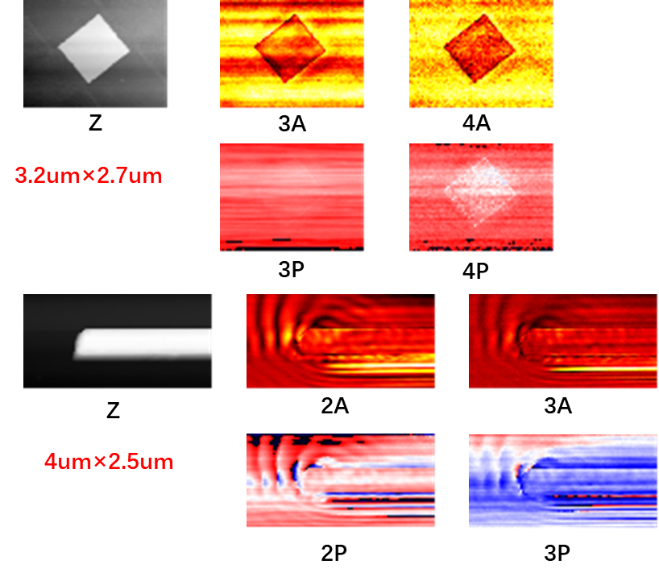
532 nm imaging: silicon calibration sample, 3 µm period, 20 nm height (top); micron dielectric waveguide (bottom)
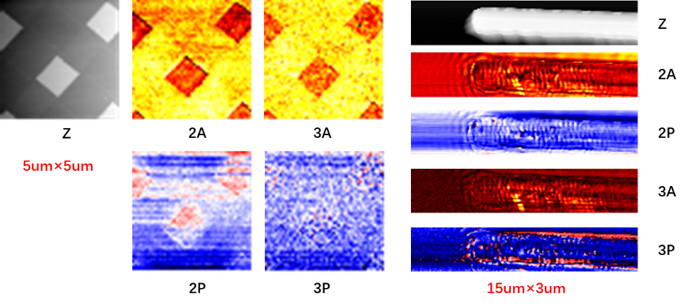
785 nm imaging: silicon calibration sample, 3 µm period, 20 nm height (left); micron dielectric waveguide (right)
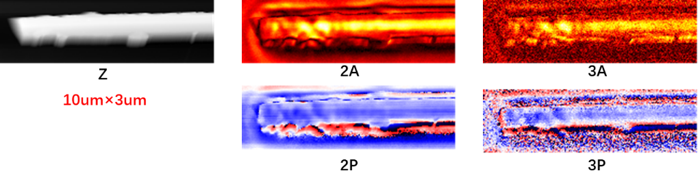
1064 nm imaging: micron dielectric waveguide
Our company has long been committed to the localization of high-end terahertz equipment and near-field optical equipment. We will continue to follow international frontier developments in related fields and publish professional interpretations of related work — stay tuned. The company currently offers terahertz far-field imaging and time-domain spectroscopy systems, terahertz near-field imaging and spectroscopy systems, and terahertz photoconductive-probe near-field systems (micron-level resolution). Researchers interested in sample testing are welcome to contact us and send samples for testing.