In 2024, Chengdu Miji Technology Co., Ltd. successfully delivered a visible/near-infrared near-field optical microscopy system to Sun Yat-sen University. The system integrates three wavelength bands: 532 nm, 633 nm and 1064 nm. The main body of the system consists of three laser sources, peripheral optical paths and a dedicated near-field atomic force main unit.
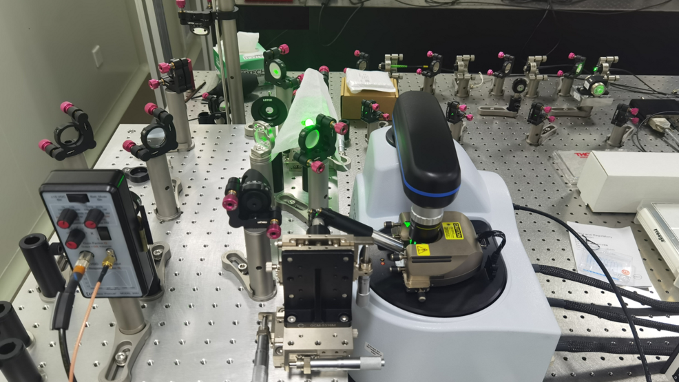
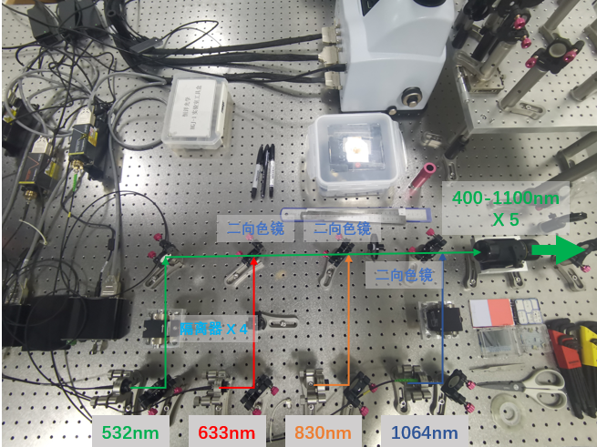
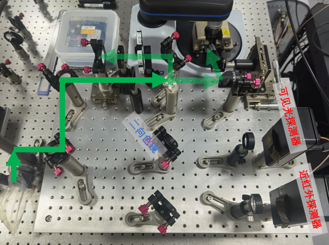
Figure 1. Visible/near-infrared near-field optical microscope
System Functions:
The system can be applied to frontier research such as polaritons in two-dimensional materials, localized electrical properties of semiconductor materials, and life sciences.
Materials science: The microscope can be used to excite polaritons in two-dimensional materials — most typically exciton polaritons in transition metal dichalcogenides (TMDs). Related work has been published in top international journals such as Nature and Nature Photonics in recent years, and many physical phenomena remain to be explored, making this field one of the current international research hotspots.
Semiconductors: SNOM is highly sensitive to the dielectric properties of samples, enabling quantitative, high-resolution and sensitive detection of doping, stress, composition and other information in semiconductor devices and nanomaterials — thereby allowing the evaluation, analysis and quality control of the composition, structure and electrical conduction properties of semiconductor materials and components at the nanoscale.
Biology: Rotational and vibrational energy levels lie in the infrared band, which can be used to quantitatively analyze chemical structure, composition and other information. By combining this system with the sensitivity of biochemical substances in the infrared and visible bands, chemical and structural characterization of organic matter, biological samples and other soft-matter materials can be performed at the nanoscale, further advancing research into the microscopic mechanisms of life sciences.
System Specifications and Imaging Results
| Light sources | 532 nm; 633 nm; 1064 nm |
| Near-field signal-to-noise ratio | 3rd-order signal: 22 dB @ 532 nm; 26 dB @ 633 nm; 22 dB @ 1064 nm |
| Spatial resolution | 40 nm |
| AFM near-field single scan range | Maximum lateral scan range: > 90 µm; maximum vertical scan range: 7.5 µm |
| Optical CCD camera | 10× objective (long working distance) • color camera, 2560 × 1920 resolution • digital zoom • 508–4010× magnification range |
| High-performance system workstation | 32 GB RAM, 2 TB storage, 3.0 GHz CPU |
1. 532 nm near-field signal and Si/SiO2 calibration sample imaging results
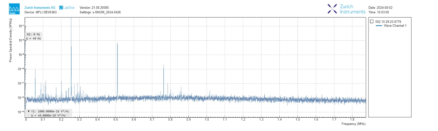
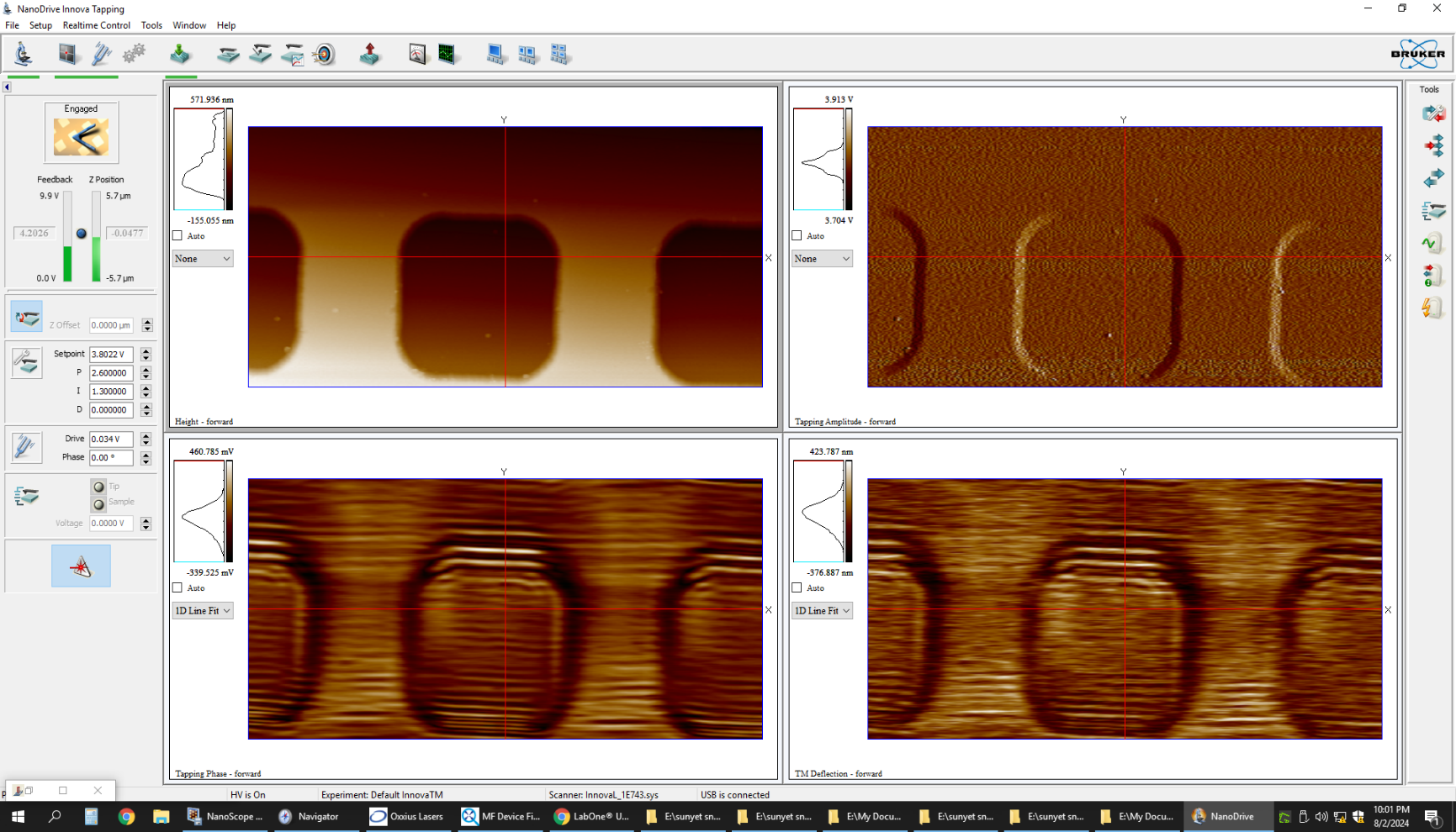
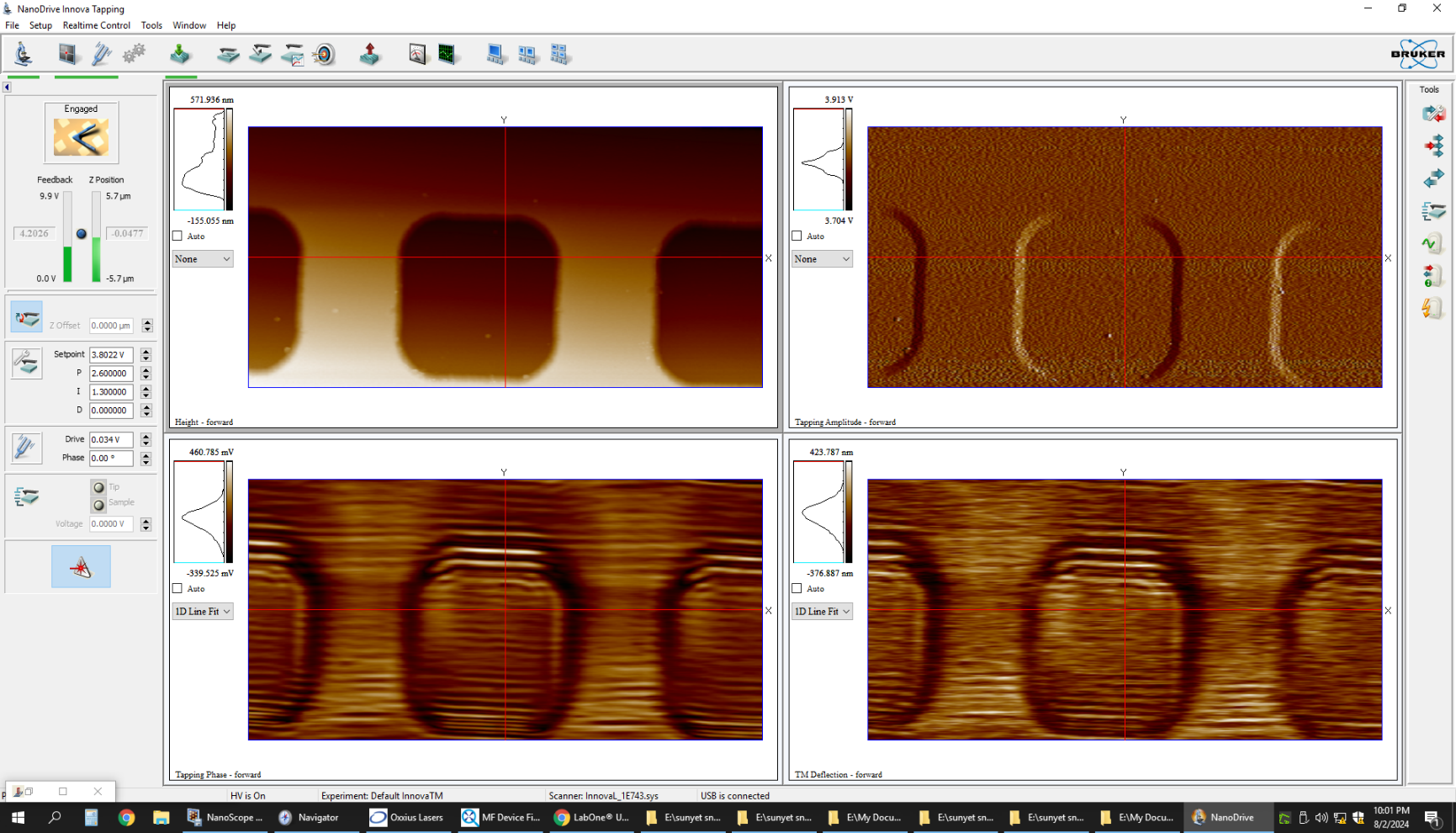
Figure 2. a and b show topography and tip voltage amplitude imaging respectively; c and d show 3rd- and 4th-order near-field amplitude imaging
2. 633 nm near-field signal and Si/SiO2 calibration sample imaging results
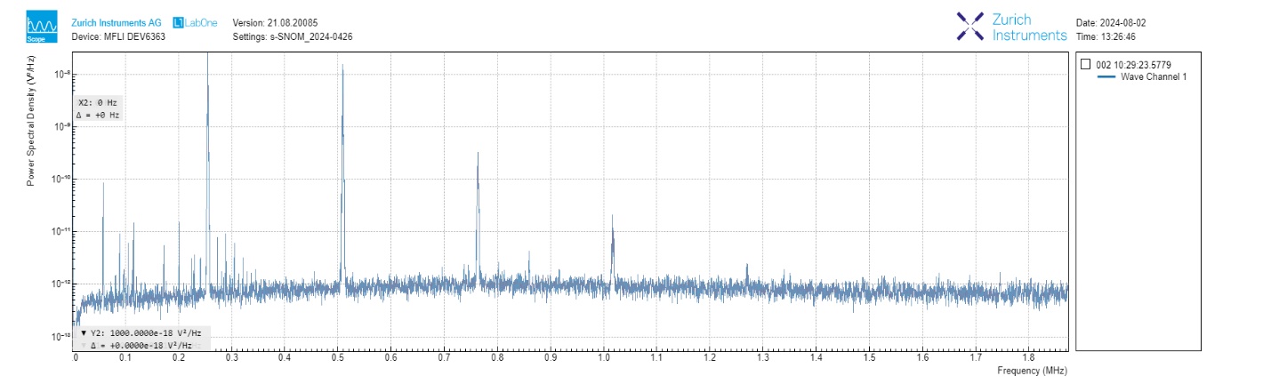
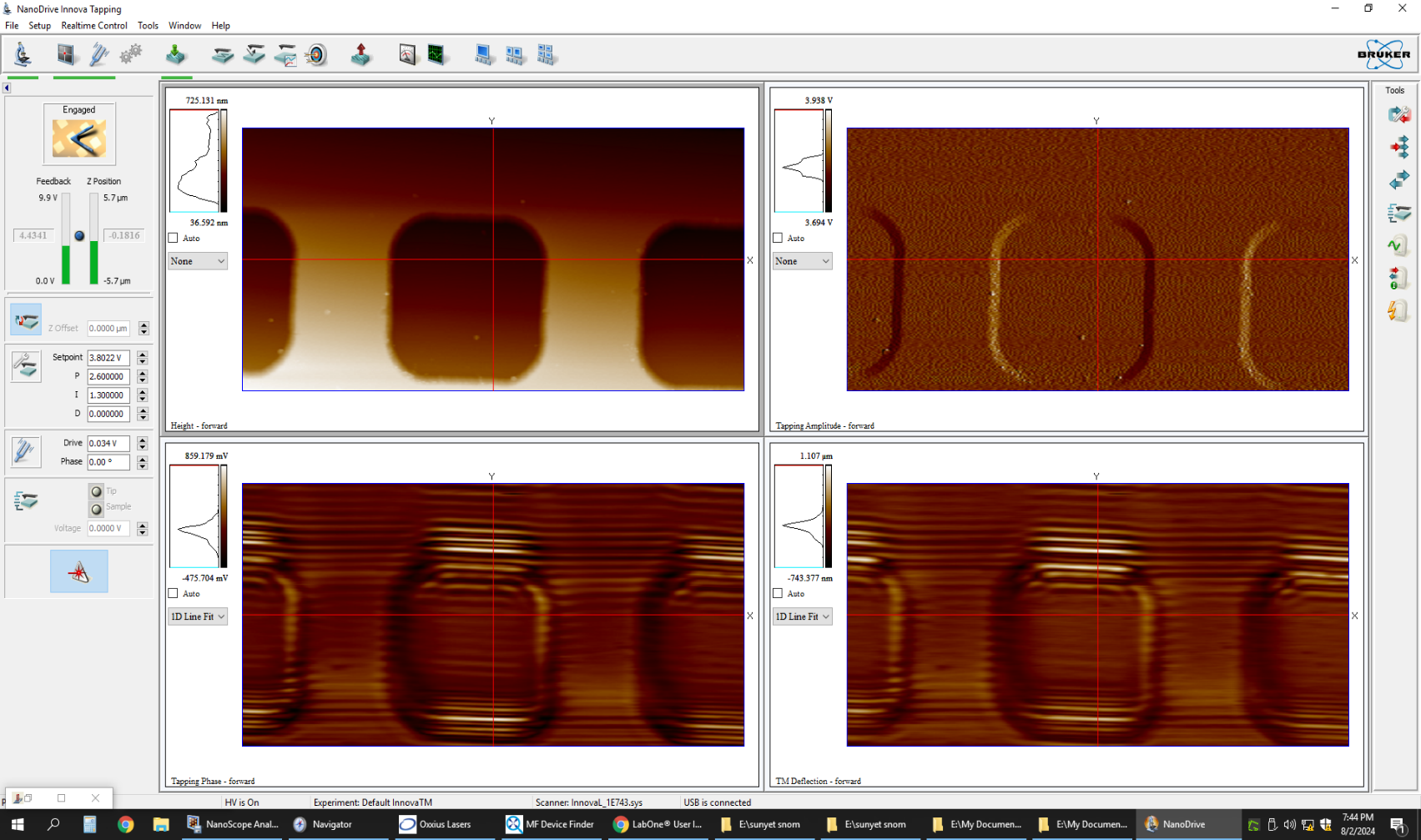
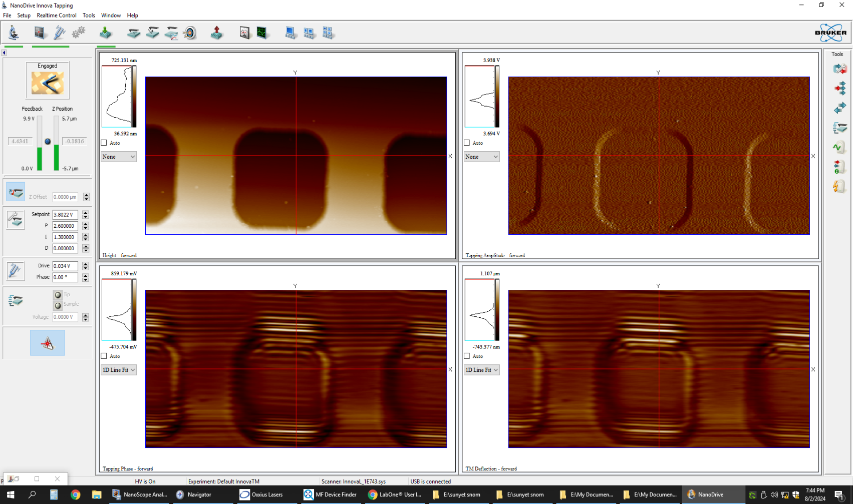
Figure 3. a and b show topography and tip voltage amplitude imaging respectively; c and d show 3rd- and 4th-order near-field amplitude imaging
3. 1064 nm near-field signal and Si/SiO2 calibration sample imaging results
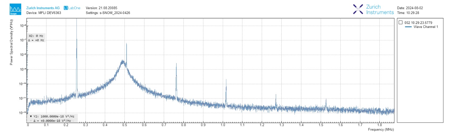
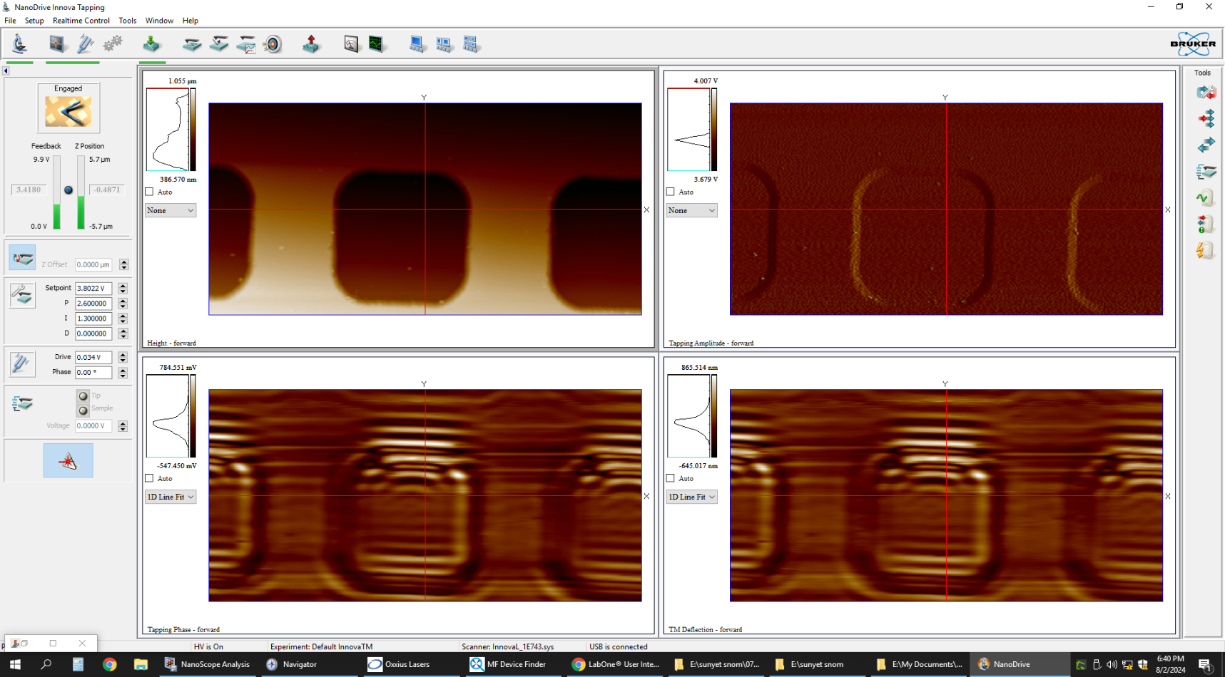
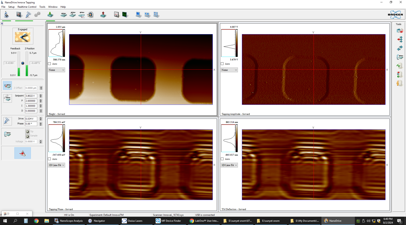
Figure 4. a and b show topography and tip voltage amplitude imaging respectively; c and d show 3rd- and 4th-order near-field amplitude imaging
Chengdu Miji Technology Co., Ltd. has long been committed to the localization of high-end terahertz equipment and near-field optical equipment. We will continue to follow international frontier developments in related fields and publish professional interpretations of related work — stay tuned. The company currently offers terahertz far-field imaging and time-domain spectroscopy systems, terahertz near-field imaging and spectroscopy systems, and terahertz photoconductive-probe near-field systems (micron-level resolution). Researchers interested in sample testing are welcome to contact us and send samples for testing.