Author: Zhang Qiyu
Background
Since the twentieth century, as Moore's law gradually approaches its physical limits, nanoscale optoelectronic integrated devices have attracted widespread attention for their advantages of high speed, low power consumption, and small size, and nanophotonics has developed rapidly. Polaritons, which enable photon manipulation at the nanoscale and the regulation of light-matter interactions, are one of the important branches of nanophotonics. Emerging two-dimensional materials provide a brand-new manipulation platform for polaritonics, and two-dimensional polaritons exhibit rich and novel physical phenomena.
Polaritons are new collective oscillation modes formed by the strong coupling of light with particles or quasiparticles in matter (electrons, phonons, excitons, magnons, etc.). These modes can break through the diffraction limit to confine free-space light within subwavelength dimensions, significantly enhancing light-matter interactions and achieving effective photon regulation at the nanoscale. The first polaritons discovered were plasmon polaritons in noble metals, produced by the interaction of photons with plasmons formed by the collective oscillation of free electrons in metals. Compared with traditional noble metals, polaritons in two-dimensional van der Waals atomic crystals possess stronger confinement capability and active tunability, with resonance frequencies covering almost the entire electromagnetic spectrum. According to material type and formation mechanism, polaritons can be divided into multiple types: plasmon polaritons in metals or doped semiconductors, phonon polaritons in polar crystals, exciton polaritons in semiconductors, and so on. These polaritons have different dispersion and propagation characteristics, and are usually closely related to the dielectric function ε [1,2].
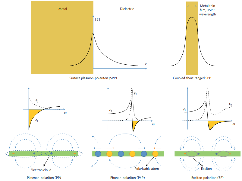
Fig. 1 Relationship between surface plasmons on metals and several typical two-dimensional polaritons [2]
Traditional optical imaging techniques are limited by the Abbe diffraction limit, with a best resolution of about half the incident wavelength, which is far from meeting the needs of studying optical phenomena at the nanoscale. The development of near-field optical imaging technology has filled this gap, the most representative being scattering-type scanning near-field optical microscopy (s-SNOM). By combining near-field optics with scanning probe microscopy, its imaging resolution no longer depends on the incident wavelength, but on the tip radius (typically on the order of tens to a hundred nanometers), enabling characterization of samples at the nanoscale. In addition, since two-dimensional polaritons have extremely strong confinement capability (kp >> k0), exciting them requires providing sufficiently large momentum compensation. In far-field experiments, momentum compensation is usually achieved by adding periodic gratings, which places extremely demanding requirements on grating structural design and fabrication precision and increases experimental complexity. In near-field experiments, however, due to the local field enhancement effect at the tip apex, s-SNOM provides a broad range of in-plane momenta — a property that makes the excitation and real-space imaging of two-dimensional polaritons possible. In recent years, a large body of work has confirmed the important role of s-SNOM in the field of two-dimensional polaritons; near-field images of polaritons help researchers more intuitively and clearly investigate novel physical phenomena and unique dispersion behaviors in two-dimensional materials. To date, s-SNOM remains the only way to obtain near-field intensity and phase information of two-dimensional polaritons [1,3].
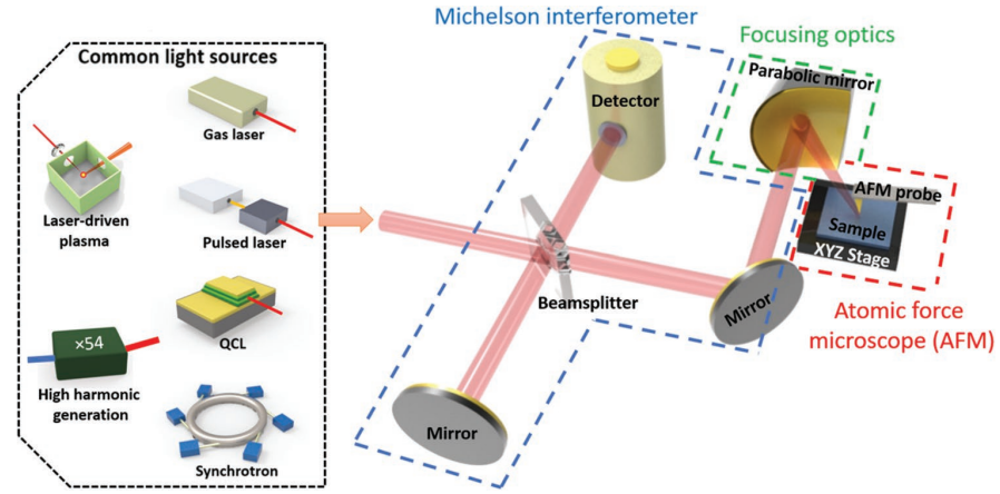
Fig. 2 Optical path diagram of a typical s-SNOM system equipped with a visible or infrared light source [3]
Applications of s-SNOM in the field of two-dimensional polaritons
Surface plasmon polaritons in graphene
Graphene has attracted widespread attention for its many unique physical properties and highly tunable advantages. In 2012, Fei et al. [4] and Chen et al. [5] separately observed plasmon polaritons in graphene using s-SNOM in the mid-infrared band (892 cm⁻¹ and 980–1086 cm⁻¹, respectively). As shown in Fig. 3a, the incident light converges at the tip and excites plasmon polaritons (wavelength λp) on the graphene surface beneath the tip. These polaritons propagate along the surface in all directions as cylindrical waves and are reflected upon encountering boundaries. The polariton waves emitted by the tip interfere with the boundary-reflected waves, forming stable periodic standing waves with a wavelength of λp/2, which are imaged point by point by s-SNOM. Experiments show that the nanoscale tip of s-SNOM can provide sufficiently large momentum to excite plasmon polaritons in graphene, and that the wavelength of the plasmon polaritons in graphene can be tuned by adjusting the back-gate voltage.
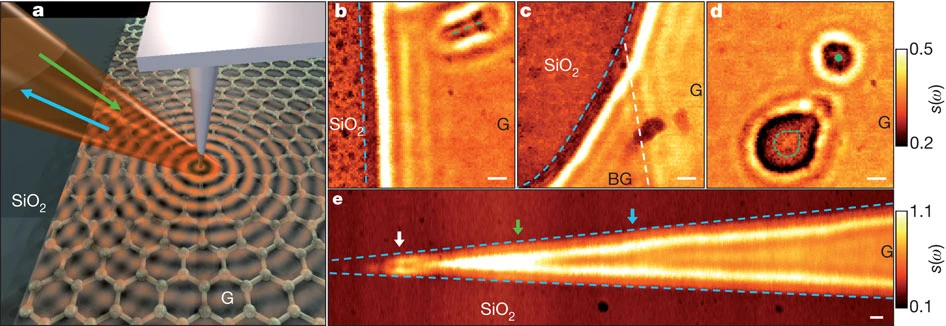
Fig. 3 Infrared nano-imaging experiment and results of graphene plasmon polaritons [4]
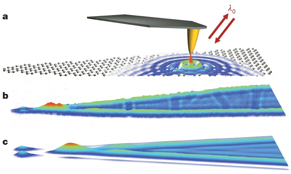
Fig. 4 Imaging propagating and localized graphene plasmons using s-SNOM [5]
Surface phonon polaritons
In 2014, Dai et al. [6] successfully observed surface phonon polaritons in the polar crystal hexagonal boron nitride (h-BN) using mid-infrared (1380–1580 cm⁻¹) s-SNOM. These polaritons are likewise reflected at boundaries and produce interference fringes with the polariton waves. Compared with plasmon polaritons in graphene, phonon polaritons in h-BN have comparable light confinement capability and lower propagation loss.
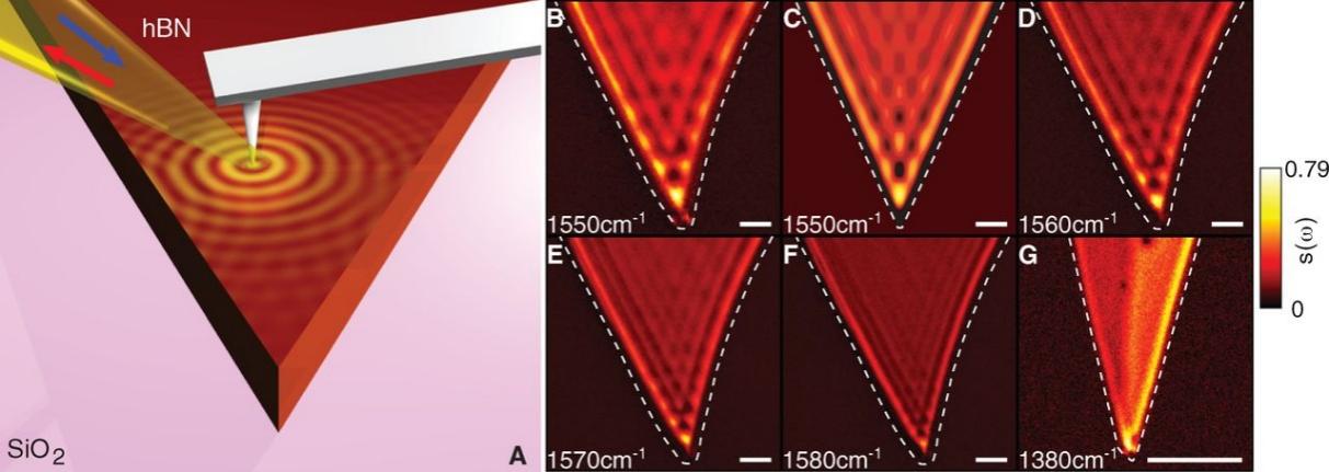
Fig. 5 Real-space imaging of h-BN surface phonon polaritons [6]
In 2018, Ma et al. [7] successfully observed surface phonon polaritons in α-MoO3 using mid-infrared (820–1010 cm⁻¹) s-SNOM. It is worth mentioning that α-MoO3 is the first two-dimensional material discovered to naturally possess in-plane hyperbolic polaritons (Fig. 6a) (εx·εy < 0). This property leads to an enhancement of the optical density of states and ray-like directional propagation along the surface, providing new ideas for photon manipulation at the nanoscale.
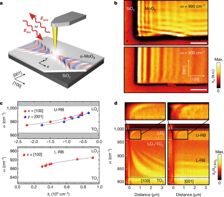

Fig. 6 Real-space imaging and nano-spectroscopy of α-MoO3 flakes, and in-plane elliptical and hyperbolic phonon polaritons in an α-MoO3 disk [7]
Exciton polaritons
In 2017, Hu et al. [8] used infrared (1.3–1.8 eV) s-SNOM to observe MoSe2, a typical representative of the TMDc material system, successfully exciting exciton polaritons and mapping their dispersion curve. They found that the exciton polaritons of this two-dimensional material are highly dependent on material thickness, and that the propagation length is very sensitive to the excitation photon energy. In addition, they discovered an interesting back-bending phenomenon in the dispersion curve.
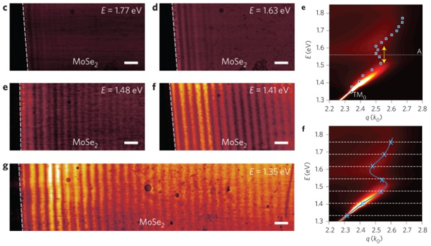
Fig. 7 Nano-optical imaging and dispersion of a MoSe2 planar waveguide [8]
In the same year, Hu et al. [9] excited MoS2 and h-BN using s-SNOM at 1530 nm and 633 nm, respectively, and deduced the permittivity of MoS2 and h-BN at specific frequencies from the interference fringe periods in the near-field images. The results show that MoS2 has strong out-of-plane anisotropy, and this work confirms the great potential of s-SNOM in characterizing the anisotropy of two-dimensional materials.
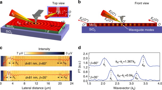
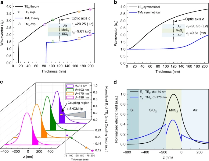
Fig. 8 Principle and results of MoS2 near-field imaging and the deduced in-plane/out-of-plane permittivity [9]
Summary
Scattering-type scanning near-field optical microscopy (s-SNOM), with its ultra-broadband optical nano-imaging technology from terahertz to visible light and its high-resolution imaging capability, has revealed many novel physical phenomena that cannot be measured by traditional optical and electronic imaging. At present, two-dimensional polaritonics is still in a stage of vigorous development. Two-dimensional materials with anisotropic polaritons provide new ideas for optical regulation at the nanoscale, and s-SNOM remains the key means of characterizing anisotropic polaritons. In addition, s-SNOM can be combined with ultrafast optics, nano-XRD, Raman, and STM to form a new generation of multimodal imaging tools for material characterization, advancing the development of condensed matter physics, chemistry, biology, and various engineering fields. It is foreseeable that in the future continuous exploration of the nanoworld, s-SNOM will surely become an indispensable tool.
References
- Zhou Yi-Xi, Li Zhi-Peng, Chen Jia-Ning. Research advances in polaritonics based on near-field optical imaging technique[J]. Acta Physica Sinica, 2024, 73(8): 080701-1-080701-21.
- Low, T., Chaves, A., Caldwell, J. et al. Polaritons in layered two-dimensional materials. Nature Mater 16, 182–194 (2017).
- Chen X, Hu D, Mescall R, et al. Modern scattering‐type scanning near‐field optical microscopy for advanced material research[J]. Advanced Materials, 2019, 31(24): 1804774.
- Fei Z, Rodin A S, Andreev G O, et al. Gate-tuning of graphene plasmons revealed by infrared nano-imaging[J]. Nature, 2012, 487(7405): 82-85.
- Chen J, Badioli M, Alonso-González P, et al. Optical nano-imaging of gate-tunable graphene plasmons[J]. Nature, 2012, 487(7405): 77-81.
- Dai S, Fei Z, Ma Q, et al. Tunable phonon polaritons in atomically thin van der Waals crystals of boron nitride[J]. Science, 2014, 343(6175): 1125-1129.
- Ma W, Alonso-González P, Li S, et al. In-plane anisotropic and ultra-low-loss polaritons in a natural van der Waals crystal[J]. Nature, 2018, 562(7728): 557-562.
- Hu F, Luan Y, Scott M E, et al. Imaging exciton–polariton transport in MoSe2 waveguides[J]. Nature Photonics, 2017, 11(6): 356-360.
- Hu D, Yang X, Li C, et al. Probing optical anisotropy of nanometer-thin van der waals microcrystals by near-field imaging[J]. Nature communications, 2017, 8(1): 1471.