Author: Yin Tinggui
At present, many two-dimensional materials have been found to possess excellent optical and electrical properties, such as graphene, MXene, transition metal dichalcogenides (TMDs), van der Waals (vdW) materials and their heterojunctions, and perovskites. They have important research and application value in terahertz modulation, detection, emission, and transmission devices, and the underlying physical mechanisms are often related to ultrafast carrier dynamics in the materials. Optical pump–terahertz probe (OPTP), as a time-resolved terahertz spectroscopy technique capable of probing ultrafast carrier dynamics of carrier excitation and recombination in materials, achieves time resolution down to the femtosecond scale (1 fs = 10⁻¹⁵ s) and has been widely applied to the study of carrier dynamics in two-dimensional materials.
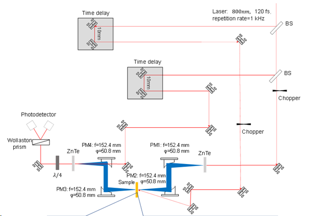
Fig. 1 A common terahertz OPTP optical path configuration [1]
As shown in Fig. 1, its working principle is to introduce, into a terahertz time-domain spectroscopy system, a high-photon-energy pump beam with adjustable time delay that excites the material (inside the blue box in the figure). Its pulse width is typically within a few hundred femtoseconds, while the terahertz wave serves as the low-photon-energy probe light. By controlling the time delay tpp between the pump and probe beams, the terahertz response of electron-hole pairs in the material from excitation to recombination can be obtained, thereby enabling the study of ultrafast carrier dynamics in materials. The video below briefly illustrates the principle and application scenarios of pump-probe technology. After years of development, OPTP has been widely applied to the study of ultrafast carrier dynamics in the two-dimensional materials mentioned above, yielding many groundbreaking and significant results.

Source: Pump-probe – Quantum made simple (toutestquantique.fr)
It is worth noting that in recent years, researchers have combined terahertz scattering-type scanning near-field optical microscopy (THz s-SNOM) with OPTP technology to achieve time-resolved terahertz spectroscopy with nanoscale resolution [3]. As shown in Fig. 2, similar to OPTP, this system introduces a pump beam into the THz s-SNOM, designing the optical path so that it is coaxial with the terahertz wave, and uses an off-axis parabolic mirror (OAP) to focus both the pump light and the terahertz onto the nanoscale tip. Exploiting the tip's local field enhancement effect and antenna resonance effect, the terahertz surface evanescent waves of the excited material at the nanoscale (with resolution determined by the tip radius of curvature) are scattered into free space, received by the receiving antenna, and near-field signals of different orders are extracted by a lock-in amplifier for studying the ultrafast carrier dynamics of materials at the nanoscale. Therefore, this system also greatly reduces the requirements on material quality and size.

Fig. 2 Structure of a terahertz near-field optical microscope with nanoscale resolution [2]
Although related research using this technology is still relatively limited both at home and abroad, this brand-new research method has already demonstrated significant advantages, as illustrated by the following examples:
Formation mechanism of depletion layers in semiconductor nanowires
Compared with semiconductor wafers, semiconductor nanowires have a large specific surface area that can improve device sensitivity, and their ease of deformation can enhance material integration capabilities. In addition, depletion layers are of great significance for semiconductor conduction and modulation, and the formation of depletion layers is closely related to the recombination of electron-hole pairs. Conventional OPTP struggles to perform precise measurements on nanowires. In 2014, M. Eisele et al. first realized time-resolved terahertz spectroscopy with 10-nanometer-level resolution and applied it to the study of carrier dynamics in InAs nanowires [3]. The study found that after excitation of the InAs nanowires, two different decay time constants appeared, and as tpp increased, the plasmon resonance frequency f0 in the terahertz near-field spectrum exhibited a red shift. Considering that f0 is positively correlated with carrier density, the authors argued that the first rapid decay process is due to the formation of the depletion layer, and the theoretically calculated depletion layer formation time agrees quite well with the experimental results.
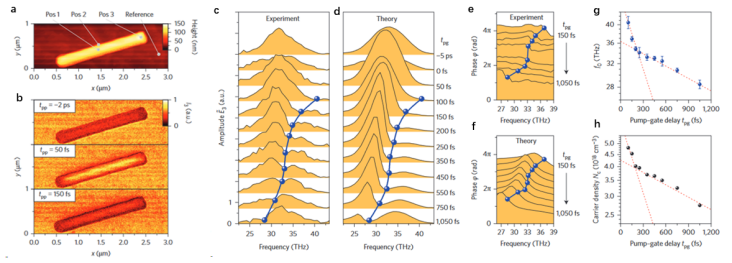
Fig. 3 Nanoscale-resolved terahertz time-domain spectroscopic microscopy results of InAs nanowires [3]
Probing tunneling processes in two-dimensional material heterojunctions: atomic-layer heterostructures have attracted widespread attention due to their unique physical properties, and interlayer electron and photon transport processes are among the key research directions. However, the limited resolution of conventional optical imaging methods makes it difficult to capture the details of these ultrafast processes. In 2021, M. Plankl et al. explored, in their work, the use of sub-cycle optical detection technology to achieve contact-free nanoscale imaging of ultrafast interlayer transport processes in atomically thin heterostructures [2]. The authors proposed using sub-cycle optical detection technology combined with time-resolved imaging, successfully achieving in-situ nanoscale imaging of electron and exciton transport processes in WS2/WSe2 heterostructures, with sub-nanometer spatial resolution and femtosecond-level time resolution. This innovative contact-free nano-imaging technique provides a new characterization means for probing ultrafast physical processes in atomic-layer heterostructures, and is of great significance for further understanding the properties of this new class of materials and developing high-performance devices based on them.
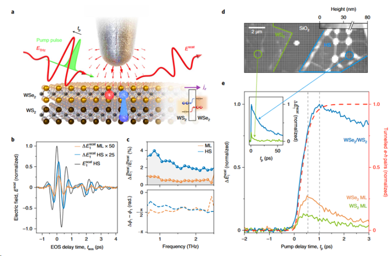
Fig. 4 Ultrafast charge transfer in a WS2/WSe2 heterojunction [2]
Exciton phase transition mechanism in two-dimensional TMD materials: in 2022, Thomas Siday et al. used ultrafast time-resolved nano-optical imaging technology [4], combined with theoretical calculations, to deeply explore the formation and evolution of high-density exciton phases in the two-dimensional material WSe2. The study found that under high exciton density conditions, WSe2 exhibits different exciton phases, including a Mott insulating phase and a metallic phase; these phase transition processes occur on picosecond ultrafast timescales and are regulated by electron-phonon coupling and electron correlation effects. Meanwhile, nanoscale imaging further revealed the spatial heterogeneity of these exciton phases. This research deepens people's understanding of exciton phase transition dynamics in two-dimensional materials and lays a foundation for developing high-performance electronic and optoelectronic devices.
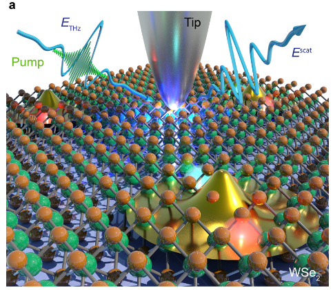
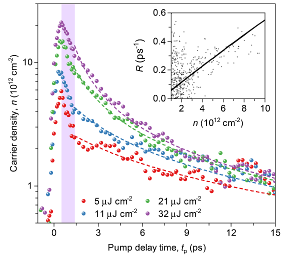
Fig. 5 Ultrafast terahertz polarization nanoscopy of monolayer and bilayer samples studying the exciton Mott transition [4]
Summary
Based on s-SNOM, this new terahertz spectroscopy technique — possessing both nanoscale spatial resolution and femtosecond-level time resolution — can non-destructively capture dynamic processes occurring ultrafast at the nanoscale, such as exciton recombination and carrier transport, providing a powerful research tool for gaining deeper insight into new materials and devices. At the same time, it offers multiple functions including time-domain and frequency-domain spectral analysis, providing comprehensive characterization information for samples. Overall, this terahertz time-resolved microscope is undoubtedly a revolutionary tool for nanoscale dynamics research and will surely play an important role in materials science, biomedicine, and other fields.
[1] Z. Jin et al., “Photoinduced large polaron transport and dynamics in organic–inorganic hybrid lead halide perovskite with terahertz probes,” Light Sci Appl, vol. 11, no. 1, p. 209, Jul. 2022, doi: 10/gqgmp3.
[2] M. Eisele et al., “Ultrafast multi-terahertz nano-spectroscopy with sub-cycle temporal resolution,” Nature Photon, vol. 8, no. 11, pp. 841–845, Nov. 2014, doi: 10/gc3jt7.
[3] M. Plankl et al., “Subcycle contact-free nanoscopy of ultrafast interlayer transport in atomically thin heterostructures,” Nat. Photon., vol. 15, no. 8, pp. 594–600, Aug. 2021, doi: 10/gj2m9w.
[4] T. Siday et al., “Ultrafast Nanoscopy of High-Density Exciton Phases in WSe 2,” Nano Lett., vol. 22, no. 6, pp. 2561–2568, Mar. 2022, doi: 10/gpk8qh.