Scattering-type scanning near-field optical microscope (s-SNOM) (also known as scattering-type scanning near-field optical microscopy, s-SNOM) can break through the diffraction limit of traditional far-field optical microscopes and obtain the local optical response of materials at the nanoscale. This capability is especially important for two-dimensional materials, strongly correlated materials, topological materials, and polariton systems, because many critical physical phenomena are not reflected solely in macroscopic averaged signals but are hidden in domain structures, boundary states, defect regions, or local phase separations.
However, many key properties of quantum materials often only emerge under extreme conditions such as low temperatures and high magnetic fields. For example, superconducting transitions, metal-insulator transitions, quantum Hall states, magnetic-field-induced topological phase transitions, and low-temperature polariton propagation all need to be studied in environments far from ambient conditions. Therefore, combining s-SNOM with low temperatures and high magnetic fields has become an important direction in the development of nano-optical characterization technology.
But this is not simply “adding a cryostat to a microscope” or “putting the sample inside a magnet.” A low-temperature, high-magnetic-field s-SNOM involves multiple challenges including optics, cryogenics, scanning probes, magnetic field compatibility, vibration control, and sample protection. This article will introduce these instrumental challenges.
Why is a low-temperature, high-magnetic-field s-SNOM needed?
In traditional transport, far-field spectroscopy, or magneto-optical measurements, what is obtained is often the averaged response across the entire sample area. For quantum materials with spatial inhomogeneity, such averaged signals may mask local differences. For instance, electrical contacts, strain, impurities, step edges, boundaries, or crystallographic domain structures can all alter the local electronic states at the nanometer or micrometer scale.
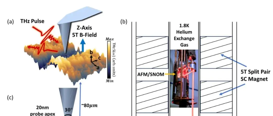
Haeuser et al.[1] reported a cryogenic, high-magnetic-field THz-sSNOM system, precisely designed to obtain local terahertz near-field responses under liquid helium temperatures and high magnetic fields. This system can operate at low temperatures and in fields up to 5 T, and was used to study the local magnetic response of the topological semimetal ZrTe₅. Compared with traditional spatially averaged measurements, the THz near-field approach can detect local responses at the nanoscale, thereby providing a new experimental means to understand spatial inhomogeneities in topological materials.
![Figure 1. Schematic of the low-temperature high-magnetic-field THz-sSNOM system[1].](https://cdn.mjthz.com/wp-content/uploads/2026/06/1786519850-wechat-17fd52fbd0d11839.png?imageView2/2/w/1200/format/webp)
The cryogenic high-magnetic-field THz-sSNOM system constructed by Haeuser et al. can operate at liquid helium temperatures and in fields up to 5 T. THz pulses enter the cryogenic chamber through a diamond window and are focused onto the region where the AFM probe interacts with the sample; the probe tip locally enhances the far-field THz light and scatters it, carrying the sample’s near-field response information.
Challenge 1: Integrating a “Nanoscale Optical Microscope” within the Magnet Bore
The first difficulty for a low-temperature, high-magnetic-field s-SNOM is space.
Conventional s-SNOM systems usually require free-space optical paths, off-axis parabolic mirrors, a probe scanning unit, a sample stage, interferometric detection optics, and detectors. The core region of a low-temperature, high-magnetic-field system is often located inside the bore of a superconducting magnet or the center of a split-coil magnet, where space is very limited. The instrument must not only fit in but also maintain stable nanometer-scale control between the probe and the sample.
Yang et al.[2] reported a low-temperature s-SNOM system operating in a temperature range of about 20–500 K and compatible with magnetic fields up to 7 T. This system adopts a compact design, integrating the AFM, sample stage, off-axis parabolic mirror, and free-space optical paths into a limited space. Since the system must simultaneously satisfy broad-spectrum illumination, a large collection angle, low-temperature compatibility, and high-magnetic-field compatibility, the overall structural design involves significant trade-offs.
This illustrates the fundamental contradiction of low-temperature, high-magnetic-field s-SNOM: on the one hand, s-SNOM requires efficient illumination of the probe tip and collection of weak scattering signals; on the other hand, the magnet bore, cryogenic chamber, and vacuum structure strongly constrain the size and placement of optical components.
![Figure 2. Compact structural design of a cryogenic s-SNOM[2].](https://cdn.mjthz.com/wp-content/uploads/2026/06/1786519850-wechat-809d25587ef07a2e.png?imageView2/2/w/1200/format/webp)
The low-temperature s-SNOM system reported by Yang et al. integrates the AFM, sample stage, probe positioning unit, and off-axis parabolic mirror within a limited space to fit inside the bore of a superconducting magnet. This design strikes a balance among space constraints, optical coupling, and mechanical stability in a low-temperature, high-magnetic-field s-SNOM.
Challenge 2: Optical Coupling and Signal Losses Caused by Cryogenic Windows
The near-field signal of s-SNOM is inherently very weak, especially in the infrared and terahertz bands. The probe scattering signal usually needs to be extracted through harmonic demodulation, interferometric detection, or time-domain sampling. Therefore, optical path efficiency greatly affects system performance.
In a cryogenic system, the light beam must pass through a vacuum window, low-temperature shielding windows, and sometimes windows made of different materials such as diamond, ZnSe, KRS-5, or quartz. Each window introduces reflection, absorption, and dispersion losses. For broadband infrared or THz systems, it is also necessary to choose appropriate window materials and detectors for the target wavelength range.
In the liquid‑helium‑temperature infrared near-field microscopy system reported by Lang et al.[3], the infrared/THz light must pass through an outer window and an inner diamond window to enter the cryogenic chamber, and then be focused onto the probe–sample region; the backscattered light returns along the same path and is collected by a detector. Depending on the wavelength, the system also needs to select detectors such as MCT, Ge:Ga, or hot‑electron bolometers.
Therefore, the optical design of a cryogenic s-SNOM must not only “illuminate the probe,” but also address a series of issues including window transmittance, optical path stability, polarization control, probe illumination efficiency, and weak signal detection.
![Figure 3. Optical path design of a cryogenic infrared/THz near-field microscopy system[3].](https://cdn.mjthz.com/wp-content/uploads/2026/06/1786519851-wechat-3e454d18b7cf3ddc.png?imageView2/2/w/1200/format/webp)
In the cryogenic infrared near-field microscopy system designed by Lang et al., infrared/THz light must sequentially pass through an outer window and an inner diamond window to enter the liquid‑helium cryogenic chamber, and then be focused onto the probe–sample region. The scattered light returns along the same path and is received by a detector, so window transmittance, optical path stability, and probe illumination efficiency all directly affect the near-field signal quality.
Challenge 3: Vibration, Thermal Drift, and Scanning Stability at Low Temperatures
s-SNOM is built on AFM, and the distance control between the probe and the sample is typically at the nanometer or even sub-nanometer scale. Vibration and thermal drift in a cryogenic system directly affect the stability of the near-field signal.
Disturbances that a cryogenic system may introduce include mechanical vibration caused by liquid helium flow or a cryocooler, mechanical drift due to thermal contraction, relative displacement between the sample stage and the probe, and changes in the piezoelectric scanning response due to temperature variations. For long‑duration scans, these factors all affect imaging quality.
In their system design, Yang et al.[2] used low‑magnetism, low‑thermal‑expansion structural components and employed independent probe and sample positioning stages to improve cryogenic imaging stability.
In cryogenic, high‑magnetic‑field THz‑sSNOM, this issue is even more pronounced. Haeuser et al.[1] specifically analyzed the influence of magnetic fields on AFM operation. They acquired AFM topography images of a ZrTe₅ sample at 0 T, 0.3 T, 1.5 T, and 5 T, and used Sobel gradient and image registration methods to evaluate the repeatability of the topography under different field conditions. These results illustrate that before discussing magnetic‑field‑induced near‑field responses, one must first confirm that the AFM can still image stably under high magnetic fields.
![Figure 4. AFM topography and gradient analysis of ZrTe₅ under different magnetic fields[1].](https://cdn.mjthz.com/wp-content/uploads/2026/06/1786519851-wechat-755c9dbc13aee287.png?imageView2/2/w/1200/format/webp)
Haeuser et al. performed AFM topography imaging on a ZrTe₅ sample at 0 T, 0.3 T, 1.5 T, and 5 T and used the Sobel gradient method to highlight surface edges and details. The repeated appearance of topographic features under different magnetic fields emphasizes the need to first verify AFM scanning stability in high‑magnetic‑field environments.
Challenge 4: Material, Structural, and Electronic Compatibility under High Magnetic Fields
High magnetic fields impose additional requirements on instrument design.
First, the materials inside the instrument should avoid ferromagnetic components as much as possible. Screws, brackets, sample holders, probe fixtures, cable shielding, and mechanical structures all need to consider magnetic‑field compatibility. Otherwise, magnetic forces, structural deformation, or vibration coupling may occur when the field is ramped up.
Second, piezoelectric scanners, translation stages, sensors, and electronic circuits may exhibit responses different from those at room temperature under low‑temperature, high‑field conditions. The scanning range, step accuracy, and closed‑loop stability can all change with temperature and magnetic field.
Haeuser et al.[1] employed a 5 T split‑coil superconducting magnet, orienting the magnetic field perpendicular to the sample surface while leaving an optical access channel for the THz light path. This configuration facilitates optical access under high magnetic fields, but further constrains the spatial layout of the AFM and optical path.
Thus, the instrument design of a low‑temperature, high‑field s-SNOM is not a single‑module optimization, but an overall balance among cryogenics, magnetic field, optical path, and AFM stability.
Challenge 5: Local Laser Heating Can Alter Cryogenic Physical Properties
In a low‑temperature experiment, “temperature” is not merely the number displayed on the temperature controller. For s-SNOM, the incident light is focused onto the probe–sample region, and the probe tip further enhances the local electromagnetic field; therefore, local photothermal effects may occur in the sample area.
Lang et al.[3] used the ferroelectric–paraelectric phase transition of the multiferroic material GaV₄S₈ to evaluate the influence of local laser heating. The results showed that, in low‑temperature near‑field experiments, the local illumination near the probe tip can cause the actual sample temperature to deviate from the sample stage temperature, thereby affecting phase transition measurements and studies of low‑energy excitations.
This is particularly important for cryogenic s-SNOM. The transition temperatures, superconducting critical temperatures, or polariton losses of many research targets are highly sensitive to temperature. If the local photothermal effect is not assessed, a “laser‑heating‑induced change” may be mistaken for an intrinsic low‑temperature material property.
Therefore, in cryogenic s-SNOM experiments it is usually necessary to control the incident optical power, spot size, sample thermal conductivity, temperature stabilization time, and the power‑dependent behavior near phase transitions.
Challenge 6: Samples May Become Brittle at Low Temperatures, and Probes May Get Contaminated
There is another easily overlooked issue in cryogenic s-SNOM: the sample itself may not withstand tapping‑mode scanning.
s-SNOM usually operates in tapping mode, in which the probe oscillates at a certain frequency near the sample surface. Although this mode is gentler than contact mode, the instantaneous local stress can still be very high given the nanometer‑scale contact area. For certain van der Waals crystals or brittle materials, the fracture toughness decreases at low temperatures, and repeated tapping by the probe may cause surface damage.
Hu et al.[4] studied this problem using α‑MoO₃ as an example. They found that low‑temperature tapping‑mode s-SNOM scanning could degrade the exposed α‑MoO₃ surface, and debris might also adhere to the probe tip, causing a decay of the near‑field signal. To address this issue, the authors proposed using few‑layer hexagonal boron nitride (hBN) as a mechanical protective layer. hBN has relatively high mechanical stability and is optically passive in the target spectral range, so it can improve the sample surface stability while minimizing interference with the phonon polariton response of α‑MoO₃.
This shows that sample preparation for low‑temperature, high‑field s-SNOM is not a simple extension of ordinary sample preparation. For brittle materials, layered materials, and polaritonic materials, protective layers, scanning parameters, probe conditions, and low‑temperature mechanical properties must all be considered together.
![Figure 5. Sample damage during cryogenic s-SNOM scanning and the hBN protection strategy[4].](https://cdn.mjthz.com/wp-content/uploads/2026/06/1786519852-wechat-9aea4e6197b7bc76.png?imageView2/2/w/1200/format/webp)
Hu et al. found that exposed α‑MoO₃ easily underwent surface degradation during low‑temperature tapping‑mode s-SNOM scanning, and debris could adhere to the probe tip, leading to near‑field signal decay. A few‑layer hBN cover layer can improve the sample surface stability while minimizing the impact on the phonon polariton response.
From Instrumental Challenges to Application Value
Although the implementation of a low‑temperature, high‑magnetic‑field s-SNOM is very difficult, the information it provides is hard to replace with traditional characterization methods.
In the study of topological materials, the magnetic field can tune the band structure, Landau levels, boundary states, and chiral transport responses. Haeuser et al.[1] applied cryogenic, high‑magnetic‑field THz‑sSNOM to ZrTe₅ and obtained local near‑field THz spectra and spatial variation information under high magnetic fields, offering a new experimental tool to study magnetic‑field‑induced responses in topological semimetals.
In strongly correlated materials, cryogenic s-SNOM can observe metal–insulator transitions, phase separation, and domain structure evolution. Yang et al.[2] used a low‑temperature s-SNOM to investigate the infrared Drude response and domain structures associated with the metal–insulator transition in VO₂ and V₂O₃, providing spatially resolved information for understanding competing phases and mesoscopic ordering.
In polariton research, low temperatures can reduce losses and alter phonon and electron excitation behaviors, making the propagation, interference, and damping processes of polaritons clearer. The study by Hu et al.[4] demonstrates that, with appropriate sample protection strategies, cryogenic s-SNOM can be further extended to phonon polariton studies of brittle van der Waals materials.
![Figure 6. Application example of cryogenic high-magnetic-field THz-sSNOM on ZrTe₅[1].](https://cdn.mjthz.com/wp-content/uploads/2026/06/1786519852-wechat-e83fd69b7d496ddb.png?imageView2/2/w/1200/format/webp)
Cryogenic high-magnetic-field THz-sSNOM can be used to probe the local near-field response of topological materials under magnetic fields. Compared with traditional transport or far-field spectroscopy measurements, this technique can further reveal nanoscale spatial inhomogeneities and magnetic-field-induced optical responses.
Summary
The core value of low-temperature, high-magnetic-field s-SNOM lies in pushing nanoscale optical imaging into the environment where critical physical phenomena in quantum materials truly occur.
The challenges it must solve are not merely “low temperature” and “high magnetic field” as two separate conditions; rather, they form a complete system‑engineering problem: how to integrate an AFM and free-space optical paths into a magnet bore, how to ensure that the infrared/THz light can still effectively illuminate the probe after passing through cryogenic windows, how to suppress the influence of vibration, drift, and magnetic field on scanning stability, how to prevent local laser heating from altering the intrinsic state of the sample, and how to protect the sample that becomes brittle at low temperatures while keeping the probe clean.
It is precisely these challenges that make low-temperature, high-magnetic-field s-SNOM not simply a microscope, but a comprehensive experimental platform facing research on quantum materials, topological states of matter, strongly correlated systems, and low-temperature polaritons.
With the continuous development of cryogenic scanning probes, broadband infrared/terahertz light sources, high-magnetic-field cryogenic systems, and nano-optical detection techniques, extreme-environment s-SNOM is expected to reveal more local physical phenomena in the future that are difficult to discover with macroscopic averaged measurements.
References
[1] Haeuser S, Kim R H J, Park J-M, et al. Analysis of Near-Field Magnetic Responses on ZrTe₅ through Cryogenic Magneto-THz Nano-Imaging[J]. Instruments, 2024, 8(1): 21.
[2] Yang H U, Hebestreit E, Josberger E E, Raschke M B. A Cryogenic Scattering-Type Scanning Near-Field Optical Microscope[J]. Review of Scientific Instruments, 2013, 84: 023701.
[3] Lang D, Döring J, Nörenberg T, et al. Infrared Nanoscopy down to Liquid Helium Temperatures[J]. Review of Scientific Instruments, 2018, 89: 033702.
[4] Hu D, Luo C, Kang L, Liu M, Dai Q. Few-Layer Hexagonal Boron Nitride as a Shield of Brittle Materials for Cryogenic s-SNOM Exploration of Phonon Polaritons[J]. Applied Physics Letters, 2022, 120: 161101.
Originally published in Chinese on the WeChat official account "见微而知著-觅几科技" (Miji Technology). English translation by Chengdu Miji Technology Co., Ltd. Source: WeChat article