PF-SNOM Nanoscale Characterization Method with Vertical Resolution and Multimodal Detection Capabilities
In the frontier exploration of micro-nano photonics and condensed matter physics, how to "see" and precisely measure the electromagnetic properties of materials at the nanoscale has long been a major challenge for scientists. Optical microscopes are limited by diffraction and cannot clearly observe the microscopic world below a hundred nanometers. Although traditional nano near-field microscopes can break the diffraction limit, they have always suffered from two major drawbacks: they cannot observe the internal near-field of materials in a layered manner, and they cannot simultaneously measure the material's hardness, softness, and electrical conductivity.
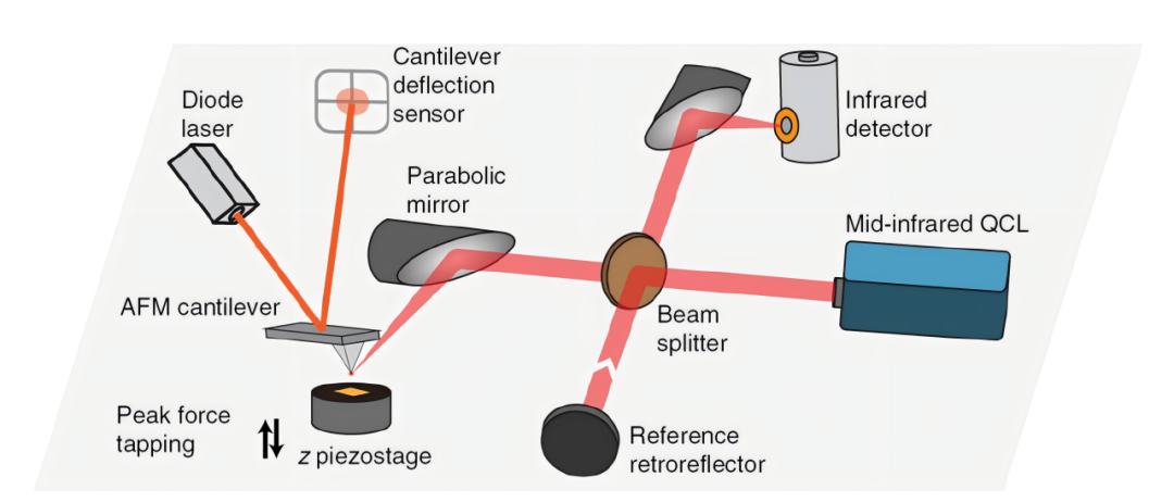
A groundbreaking study published in *Nature Communications* in 2018 introduced a novel technique called peak-force scattering-type scanning near-field optical microscope (PF-SNOM). This technology revolutionizes nano-optical characterization, enabling not only nanoscale three-dimensional tomography but also the simultaneous acquisition of optical, mechanical, and electrical information in a single scan, opening a new door for high-precision near-field nanometrology in the future.
Traditional scattering-type scanning near-field optical microscope (s-SNOM) has driven the rapid development of nano-optics over the past decade. However, as research deepens, its inherent limitations have become increasingly prominent:
Loss of Distance Information and "Artifacts": Traditional s-SNOM relies on tapping mode and higher harmonic demodulation techniques to extract near-field signals. As the probe rapidly taps the sample surface, it becomes difficult to precisely determine the absolute distance between the probe tip and the sample. This loss of distance information not only prevents the reconstruction of three-dimensional optical field distributions but also easily introduces topographic artifacts on sample surfaces with significant undulations.
Difficulty in decoupling multiple physical fields: In traditional tapping mode, the probe operates in a state of high-frequency oscillation, preventing researchers from simultaneously performing near-field optical imaging and mechanical or electrical measurements that require stable contact between the probe and the sample.
Quantitative extraction error of the dielectric constant: The lack of precise tip-sample distance parameters introduces non-negligible fitting errors in traditional dipole models, making it difficult to achieve high accuracy when extracting the complex dielectric constant of unknown materials.
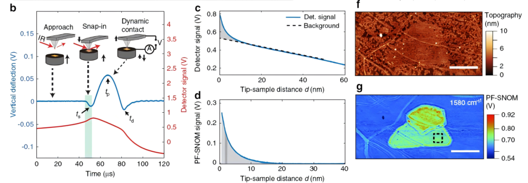
c. Relationship between the infrared detector signal and the probe-sample distance d, derived from the two waveforms in b.
d. The pure near-field signal with clear distance dependence is obtained by subtracting the linear background fitted in c.
f. Topography of the graphene region grown by chemical vapor deposition on a SiO₂ substrate. g. PF-SNOM image of the graphene region in the 1580 cm⁻¹ infrared band.
To overcome the above bottleneck, the research team proposed an ingenious design concept: keep the probe stationary while moving the sample. In PF-SNOM mode, the cantilever of the probe no longer oscillates actively; instead, the sample stage below performs low-frequency vertical reciprocating motion with a large amplitude (e.g., 300 nm). At the moment when the sample approaches extremely close and contacts the probe, the system utilizes highly sensitive optical deflection technology to precisely capture the "Peak Force" exerted on the probe tip, using it as the feedback signal.
Meanwhile, by integrating time-gated optical detection technology, the system can precisely capture light scattering signals at different absolute heights from the retraction curve as the probe-sample distance gradually increases from zero. Through real-time calculation and subtraction of the far-field background, it achieves an exceptionally pure near-field optical response.
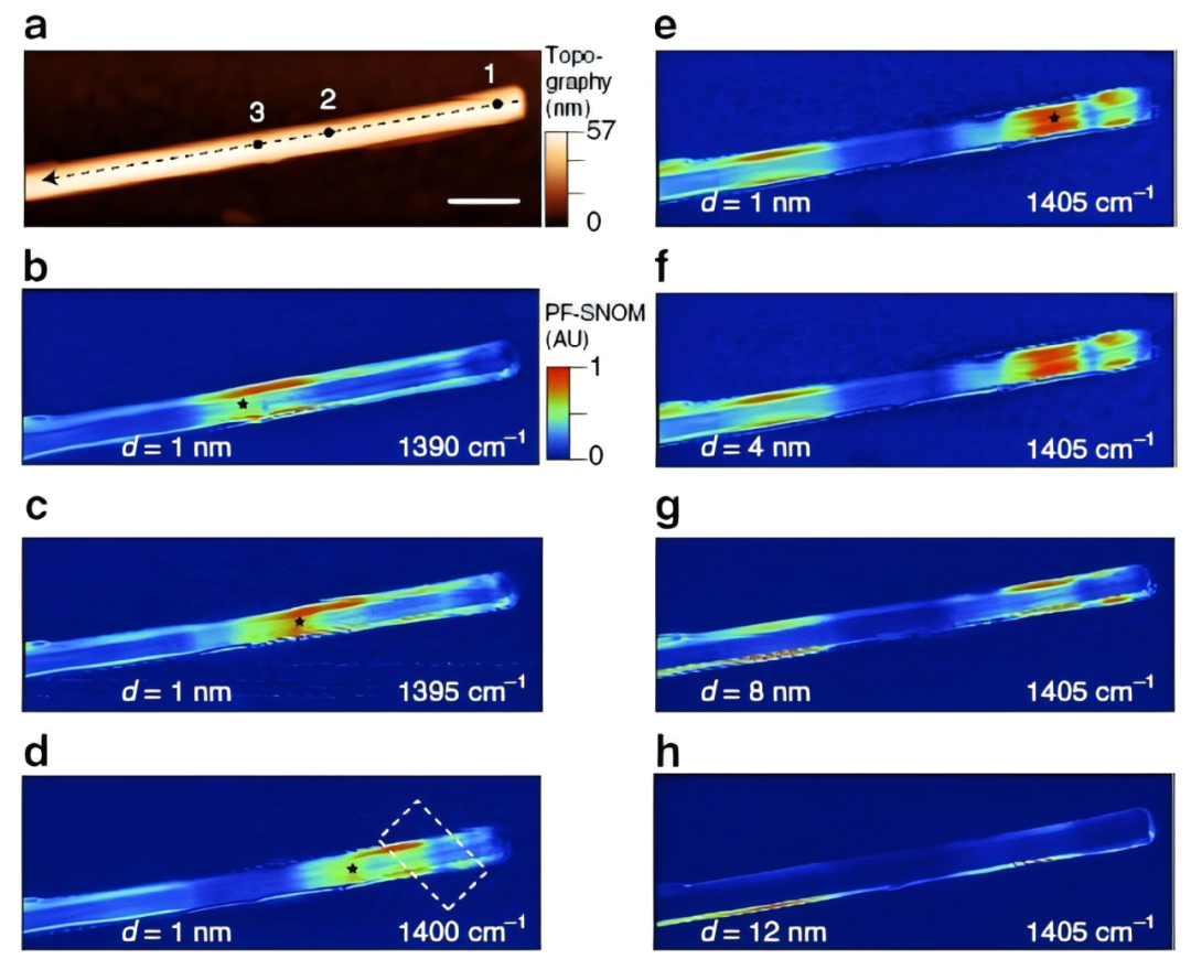
b–h. Normalized peak-force scattering-type scanning near-field optical microscope (PF-SNOM) imaging of boron nitride nanotubes.
Thanks to precise control over absolute distance, researchers can arbitrarily extract optical slices at distances of 1 nm, 4 nm, or even more than 10 nm from the sample surface. In the observation of phonon polaritons in two-dimensional materials (such as boron nitride nanotubes, BNNTs), PF-SNOM clearly reveals the exponential decay behavior of the polariton field in three-dimensional space. This high-precision distance control also provides extremely important data support for future depth inversion of subsurface nanostructures.
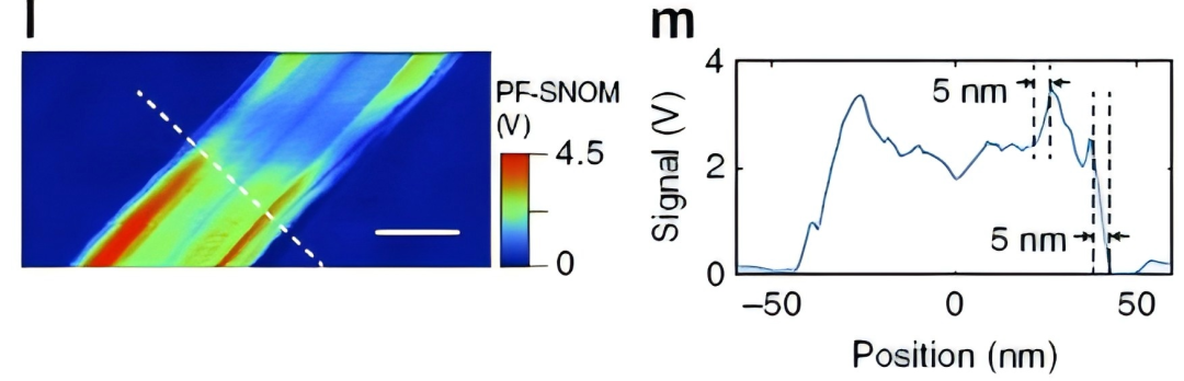
m. PF-SNOM signal intensity distribution curve taken along the white dashed line in Figure I, showing that the instrument achieves a spatial resolution of up to 5 nm.
Previously, the resolution of s-SNOM was typically limited by the probe's curvature radius. However, at extremely close distances (< 2 nm), a highly localized "gap mode" forms between the tip and the sample. PF-SNOM can stably extract signals at such extremely close distances, dramatically improving spatial resolution to an astonishing 5 nm, making even the smallest lattice defects and local field variations clearly visible.
The performance of microelectronic devices (such as thin films and structures in micro/nano fabrication) is often the result of multi-physics coupling. PF-SNOM enables simultaneous acquisition of near-field optical phase/amplitude, elastic modulus, surface adhesion, and contact conductivity of materials in a single scan. This multimodal integration provides a comprehensive solution for the inspection of complex micro/nano devices.
Moving from qualitative observation to high-precision quantitative measurement is an inevitable trend in the development of nano-optics. With its unparalleled absolute distance control and multi-physics synchronous imaging capabilities, PF-SNOM technology not only resolves the long-standing issues of artifacts and multimodal incompatibility in the near-field optics field but also lays a solid experimental foundation for establishing universal and high-precision near-field quantitative inversion models.
References
Wang, H.; Wang, L.; Jakob, D. S.; Xu, X. G. Tomographic and Multimodal Scattering-Type Scanning near-Field Optical Microscopy with Peak Force Tapping Mode. Nat Commun 2018, 9 (1), 2005.

Originally published in Chinese on the WeChat official account "见微而知著-觅几科技" (Miji Technology). English translation by Chengdu Miji Technology Co., Ltd. Source: WeChat article