Author: Zhang Siyuan
As early as 1887, Hertz observed the photoelectric effect. Subsequently, Einstein explained this phenomenon through quantum theory in 1905, which not only won him the Nobel Prize, but also opened the door to modern physics. For a century, photoemission technology (shining light on a solid to excite electrons) has been a core cornerstone of quantum material analysis, night vision detection, particle accelerators, and ultrafast microscopy.
However, traditional photoemission technology has always faced a troublesome "physical mismatch" problem. Recently, a research team from the University of Southern California and Arizona State University published a breakthrough study in Nano Letters, using a brand-new "Evanescent Mode Photoemission" (EMP) mechanism that completely rewrites the rules of the game in this field.
1. Solving the century-old "absorption-escape" contradiction
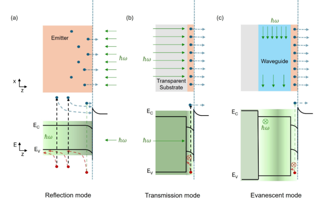
In traditional photoemission, light is mainly incident in two ways:
● Reflection Mode: light shines on the material from the front, and electrons fly out from the same side.
● Transmission Mode: light passes through the substrate from behind, exciting electrons at the front.
Where does the problem lie?
The absorption depth of light in solid materials is typically between 100 nm and 1 μm, but the "mean free path" over which excited electrons can escape alive is only a few tens of nanometers. This means that most electrons generated by photons are trapped deep inside the material and cannot be utilized. To get the electrons out, we have to make the film extremely thin, but this in turn leads to insufficient photon absorption and greatly reduced efficiency.
2. A clever trick: letting light travel parallel to the surface
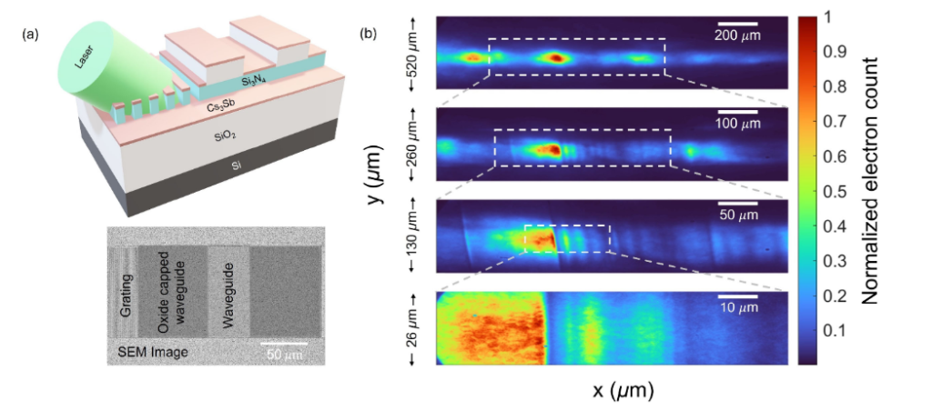
The research team proposed a highly creative solution: instead of letting light "strike" the surface perpendicularly, they let it propagate in parallel within a silicon nitride (Si₃N₄) waveguide beneath the emission layer.
● Physical mechanism: although the light is confined within the waveguide, its "shadow" — the evanescent wave — extends outside the waveguide and is absorbed by the cesium antimonide (Cs₃Sb) thin film above, which is only 5 nm thick.
● Efficiency revolution: this approach completely decouples the "light absorption depth" from the "electron escape depth". The absorption length of light now depends on the axial length of the waveguide rather than its thickness, which enables even a 5 nm ultrathin layer to achieve an extremely high emission yield.
3. "Seeing" photons, shaping electrons
The research team used photoemission electron microscopy (PEEM) to capture these emitted electrons in real time. Amazingly, the electron beams perfectly present a "self-portrait" of the optical modes inside the waveguide.
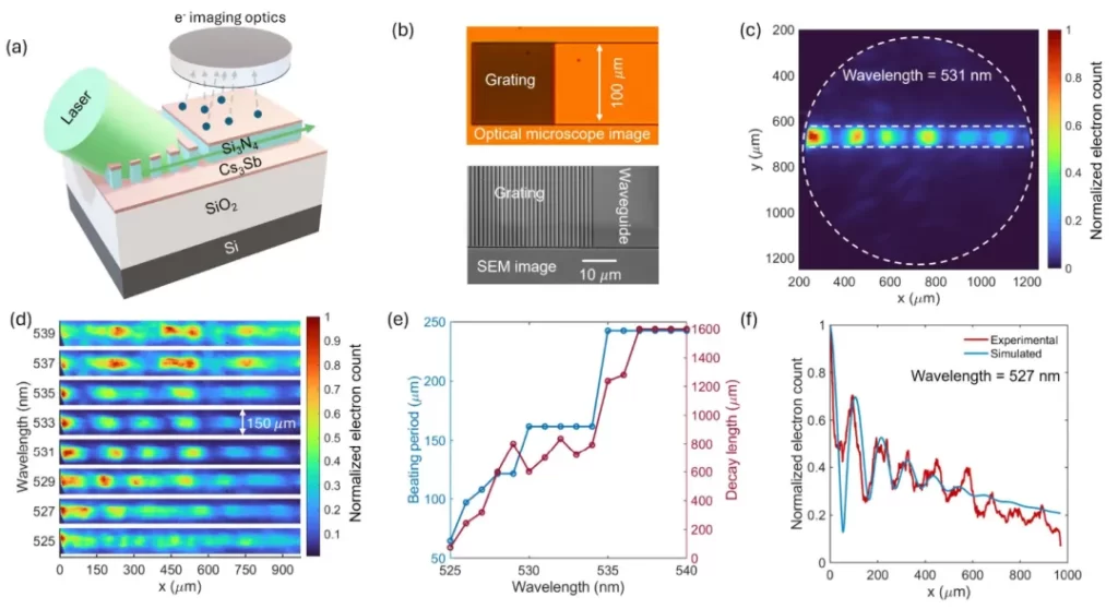
Through this technique, the scientists achieved two unprecedented capabilities: ● Direct imaging of optical fields: mode interference inside the waveguide can be directly observed at micrometer and even millimeter scales, with nanoscale resolution.
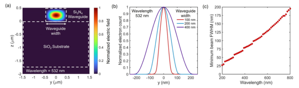
● Precise shaping at the source: by adjusting the width of the waveguide, electron beams of specific shapes can be "pinched" directly at the emission source.
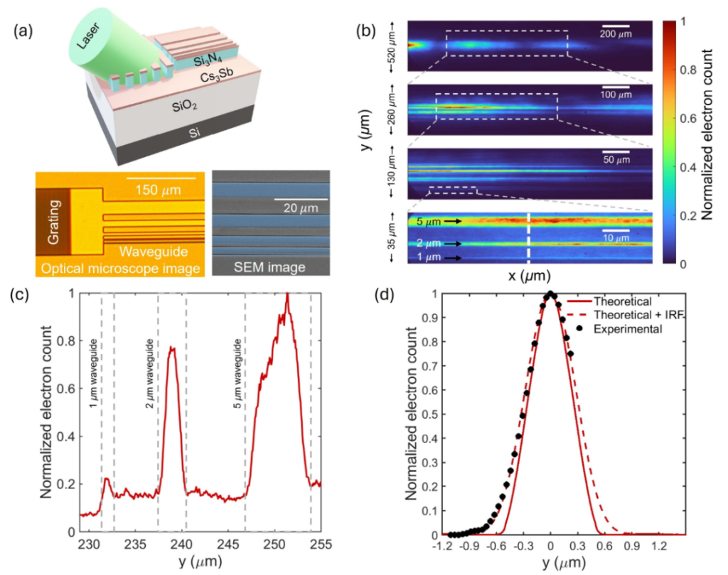
Experiments demonstrate that the current transverse features of the electron beam can be confined below 600 nm. Theoretical calculations further indicate that when using short-wavelength (e.g., 235 nm) lasers, the electron beam can be compressed to an astonishing 40 nm width.
4. Future possibilities: from electronic chips to femtosecond cameras
This technology is not only a breakthrough in physical theory, but also has broad application prospects.
By adding specific silicon dioxide (SiO₂) cladding layers on the waveguide, the researchers can even artificially modulate the texture of the electron beam, achieving complex pattern engineering.
● Maskless electron beam lithography: in the future, expensive masks may no longer be needed — nanochips could be directly "printed" through photonic networks.
● Ultrafast electron microscopy: using femtosecond pulse lasers, electron pulses highly correlated in time and space can be generated to capture instantaneous processes at the nanoscale.
● Particle accelerators: providing higher-brightness electron sources for free-electron lasers and particle colliders.
Summary: Evanescent-mode photoemission tightly integrates photonics, materials science, and ultrafast electronics, opening a new window for precise manipulation of the nanoworld.
References:
Ahsan, R., et al. (2025). Evanescent Mode Photoemission. Nano Letters, 25(4), 15487-15494. https://doi.org/10.1021/acs.nanolett.5c03185