Author: Zhang Tianyu
Recently, the research teams of Liu Ming and Yan Ruoxue from the University of California, Riverside (UCR) jointly developed 3D photocurrent nano-imaging technology with 4 nm spatial resolution, and for the first time observed a micrometer-scale (>1 μm) region dominated by the photothermoelectric effect (PTE) in a MoS₂-Au Schottky diode — overturning the conventional understanding that photocurrent is mainly confined to the electrode interface. Through harmonic demodulation and background subtraction techniques, the contributions of the photovoltaic effect (PV) and PTE were successfully separated, and it was found that hexagonal boron nitride (h-BN) encapsulation can enhance the PTE current by up to 6 times (from -0.5 nA to -3 nA) through lateral heat diffusion. The study provides a new paradigm for the design of 2D material optoelectronic devices, revealing the key influence of spatial modulation of the Seebeck coefficient in 2D materials under weak electrostatic screening on the photoresponse.
This research was published in the internationally renowned academic journal Science Advances under the title "Deciphering photocurrent mechanisms at the nanoscale in van der Waals interfaces for enhanced optoelectronic applications". The corresponding authors are Liu Ming and Yan Ruoxue, and the first author is Xu Da.
Research background
1. Bottlenecks of traditional techniques:
1) The optical diffraction limit restricts the spatial resolution of traditional photocurrent microscopy (such as SPCM) to λ/2 (~300 nm), making it unable to resolve nanoscale photoresponse mechanisms.
2) In 2D materials, the PV effect (photogenerated carrier separation) and the PTE effect (temperature-gradient-driven current) often coexist and are difficult to distinguish with traditional methods; for example, PTE currents in graphene can only be observed over a range of 100–200 nm.
2. Challenges of the MoS₂-Au heterojunction:
1) The photocurrent of Schottky diodes is traditionally attributed to the PV effect at the interface, but thermal management issues are prominent: 2D materials have low thermal conductivity (MoS₂ about 34.5 W/mK), and the temperature gradient after light absorption is easily overlooked.
2) How the thermal conductivity anisotropy of encapsulation layers (such as h-BN: 600 W/mK in-plane, 5 W/mK out-of-plane) affects heat diffusion and the PTE response remains unclear.
3. Key scientific gaps:
1) Does weak electrostatic screening in 2D materials lead to an expanded range of Seebeck coefficient spatial modulation?
2) How can experimental techniques simultaneously quantify the nanoscale distributions of PV and PTE?
Research objectives
1. Technical breakthrough: develop a 3D near-field photocurrent imaging system with 4 nm spatial resolution to separate PV and PTE effects.
2. Mechanism revelation: elucidate the micrometer-scale extension mechanism of the PTE effect at the MoS₂-Au interface, and quantify the influence of weak electrostatic screening on Seebeck coefficient modulation.
3. Material optimization: verify the enhancement effect of h-BN encapsulation on lateral heat diffusion and improve PTE current efficiency.
Research content and results
Fig. 1 shows the cross-sectional structure of the core experimental device.
A 10 nm thick few-layer MoS₂ flake was transferred onto pre-deposited gold electrodes (30 nm Au/2 nm Cr) via a capillary-force-assisted clean transfer method, forming a dual Schottky barrier (SB) photodiode. The device substrate is a 290 nm SiO₂/Si wafer, with the silicon substrate serving as a back gate to tune the electron doping level of the MoS₂. To protect the MoS₂ from oxidation and laser ablation and to optimize thermal management, the entire structure was encapsulated with a 5 nm thick h-BN layer. This transfer method avoids the introduction of chemical disorder and defect states, making the SB height of the source and drain electrodes approach the Schottky-Mott limit and ensuring the purity of the interfacial electrical properties.
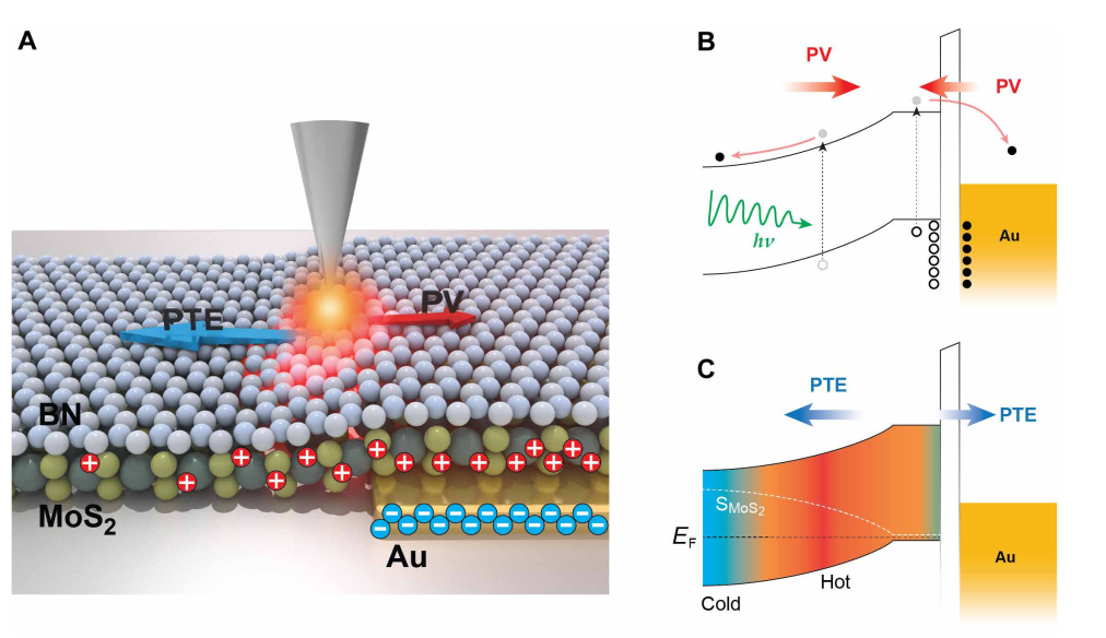
Fig. 2 systematically presents the experimental setup and data processing workflow.
Fig. 2A shows the experimental setup: a 671 nm continuous-wave laser, after modulation (~10 Hz), is coupled into an optical fiber, and ultra-focusing (spot size ~5 nm) is achieved through a tapping-mode AFM probe (oscillation frequency 32 kHz). A silver nanowire (AgNW) protruding 5 μm from the probe tip ensures mechanical stability. During scanning, the laser and probe motion are synchronized via an optical chopper; 8 data points are collected per pixel (4 light on/off cycles), the lock-in amplifier (LIA) integration time is 10 ms, and the photocurrent signal is separated through harmonic demodulation (orders 1–6).
Fig. 2B-D show the key data processing steps: the photocurrent waveform (IPC(t)) is reconstructed via Fourier series and correlated with the sinusoidal motion of the probe (z(t)) to obtain the approach curve (IPC(z)). The curve shows an inflection point at 10–20 nm, indicating the coexistence of two mechanisms: the photovoltaic effect (PV) dominates in the near field (<10 nm) due to evanescent field enhancement, while the photothermoelectric effect (PTE) contributes significantly in the intermediate near field (10–20 nm) due to heat diffusion.
Fig. 2E-G fit the PV/PTE characteristic curves through multiphysics simulations and separate the two contributions using linear least squares. For example, in the electrode edge region, the PTE current accounts for 65% of the total current, while PV accounts for only 35%.
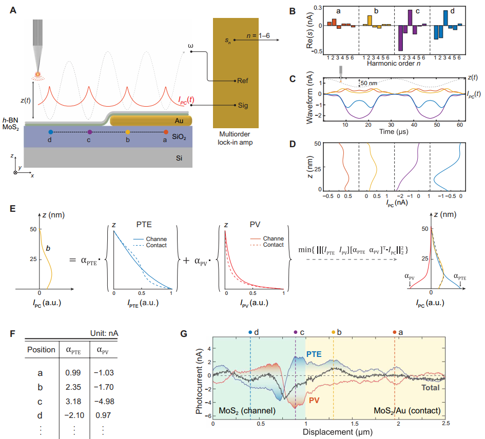
Fig. 3 reveals the generation mechanisms of PTE and PV currents through the band structure.
Fig. 3A-B show that a van der Waals gap (vdW gap) exists between the MoS₂ and the Au electrode, forming an additional tunneling barrier superimposed on the intrinsic Schottky barrier. Fig. 3C-F show the band bending under different VDS and VGS:
Positive VDS + negative VGS (Fig. 3E-F): intrinsic electrons in the MoS₂ are depleted, and the depletion region extends to 1 μm, leading to enhanced spatial modulation of the Seebeck coefficient (S) and a significant increase in PTE current (IPTE = ∫-S▽Tdx); meanwhile, the enhanced electric field promotes photogenerated carrier separation, and the PV effect is simultaneously enhanced.
Negative VDS + positive VGS (Fig. 3D): the band bending weakens, the S gradient concentrates at the electrode edge, and both PTE/PV currents are confined to a narrow region (<200 nm).
Fig. 3G intuitively shows how the product of S(x) and the temperature gradient (dT/dx) drives the PTE current: regions where S(x) decreases monotonically produce negative current, while increasing regions produce positive current, verifying the applicability of the Mott relation (S ∝ d(lnσ)/dE) in 2D materials.
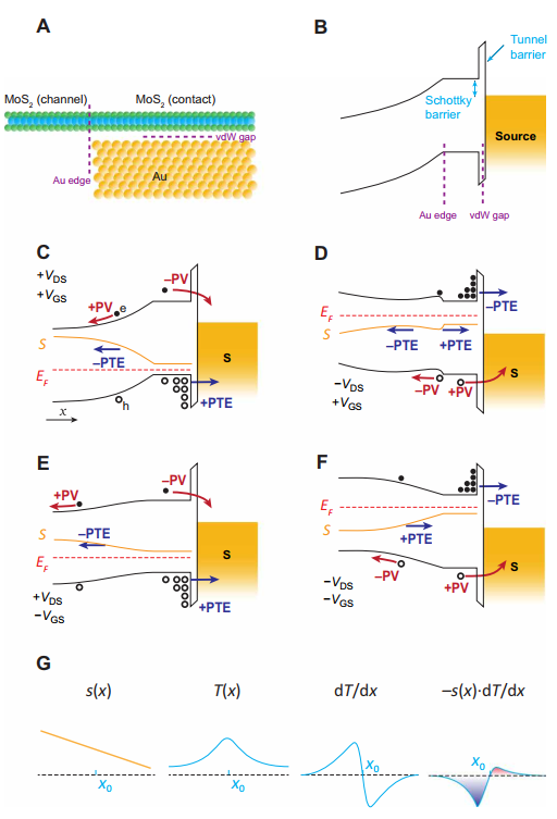
Fig. 4 compares the distributions of total current, PTE, and PV components under different gate voltages (VGS = +25 V, -5 V, -20 V).
VGS = +25 V (Fig. 4A): the MoS₂ is highly electron-doped, the depletion region is narrow (~200 nm), the PTE current is confined to the electrode edge, the PV effect is suppressed due to enhanced carrier recombination, and the total current is only -0.3 nA.
VGS = -20 V (Fig. 4C): electron depletion causes the depletion region to extend to 1 μm; the slowly varying S(x) expands the integration region of the PTE current, while the high-resistance channel enhances the electric field, boosting the PV current to 0.5 nA and the total current to -3 nA (a 10-fold increase compared to +25 V).
Fig. 4D-E verify the experimental results through simulations: under weak band bending (positive VGS), the PTE current exhibits a narrow peak distribution; under strong bending (negative VGS), the current distribution broadens and its amplitude increases. Fig. 4F fits the carrier concentration based on a parallel-plate capacitor model, yielding a charge neutrality point VCNP = -27 V, consistent with the experimentally measured variation of the depletion region width.
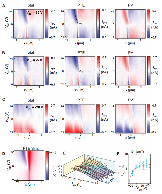
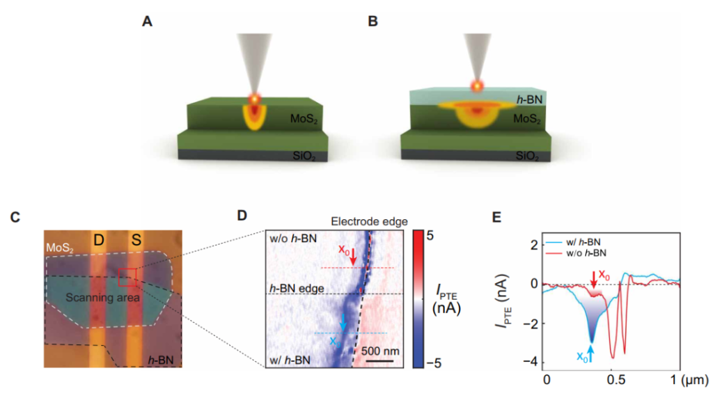
Fig. 5 reveals the thermal management role of h-BN.
Fig. 5A-B show through finite element simulations that without h-BN, the hot spot generated by light absorption has a FWHM of only 20 nm; after encapsulation, the high in-plane thermal conductivity of h-BN (600 W/mK) promotes lateral heat diffusion, expanding the hot spot FWHM to 150 nm and tripling its overlap with the Seebeck coefficient gradient region (1 μm).
Fig. 5C-E provide experimental verification: in devices partially covered with h-BN, the PTE current in the encapsulated region reaches -3 nA, while that in the bare region is only -0.5 nA — an enhancement of 6 times. The hot spot expansion significantly increases the PTE current integral (VPTE ∝ ∫Tdx), while the insulating properties of h-BN reduce leakage current. This result directly demonstrates the feasibility of regulating the PTE response through heat diffusion with high-thermal-conductivity encapsulation layers.
Summary and outlook
This study not only breaks through the spatial resolution limit of photocurrent imaging, but also reveals the core role of thermal management in 2D material optoelectronic devices, providing quantitative guidelines for the design of high-efficiency photodetectors.
Core conclusions:
1. Technical level: the 3D photocurrent nano-imaging technology achieves 4 nm resolution, providing a brand-new tool for studying nanoscale photoresponse mechanisms.
2. Mechanism level: weak electrostatic screening in 2D materials causes the PTE effect to extend beyond 1 μm, with spatial modulation of the Seebeck coefficient being the key driving factor.
3. Application level: h-BN encapsulation enhances the PTE current by 6 times through lateral heat diffusion, providing a quantitative basis for the design of high-thermal-conductivity encapsulation layers.
Future directions:
1. Device optimization: tune the h-BN thickness (5–20 nm) and the number of MoS₂ layers to further improve heat diffusion efficiency.
2. Material extension: apply the technique to other 2D heterojunctions (such as WS₂/WSe₂) to explore the influence of interlayer coupling on PTE.
3. Functional integration: combine low-temperature (4 K) and time-resolved (ps-level) measurements to study the contribution of exciton dynamics to photocurrent.
Paper information
Da Xu et al., Deciphering photocurrent mechanisms at the nanoscale in van der Waals interfaces for enhanced optoelectronic applications. Sci. Adv. 11, eadv7614 (2025). https://www.science.org/doi/full/10.1126/sciadv.adv7614