Author: Yu Shuchao
Nanotechnology is a technology for studying and applying the properties of materials at the nanoscale. For nanoscale observation, we need a series of powerful microscopes. Among them, the Scanning Tunneling Microscope (STM) and the Atomic Force Microscope (AFM) are the most widely used microscopes at the nanoscale.
If a certain bias voltage is applied across two metal electrodes, when the gap between them reaches a few nanometers or even smaller, some electrons will penetrate the potential barrier, forming a weak current between the tip and the sample — this phenomenon is called the tunneling effect. STM was developed based on the tunneling effect. Compared with STM, AFM observes by detecting the atomic forces between the probe tip and the sample under test, which is superior to STM's current-based detection because it can be used not only for semiconductors but also for insulators. Through a feedback mechanism, the force generated as the probe tip approaches the sample surface is kept at a constant level, thereby producing the atomic force microscope image. [1]
The basic principle of AFM is shown in Fig. 1. [2] A probe capable of detecting weak forces is positioned at the surface of the sample under test, with a reflective mirror on its back. A laser beam is directed onto the probe by a laser, and the reflected laser enters a four-quadrant position-sensitive detector (PSD). At this point, if something changes between the probe tip and the sample, the tip-sample interaction force will change, causing the micro-cantilever to deform, and the light spot reflected into the PSD will shift. AFM exploits the weak interaction force between the probe tip and the sample surface to deform the micro-cantilever, controls the constancy of the sample-tip interaction force through a feedback loop, and detects the deformation of the micro-cantilever by various methods to obtain the surface topography information of the sample.
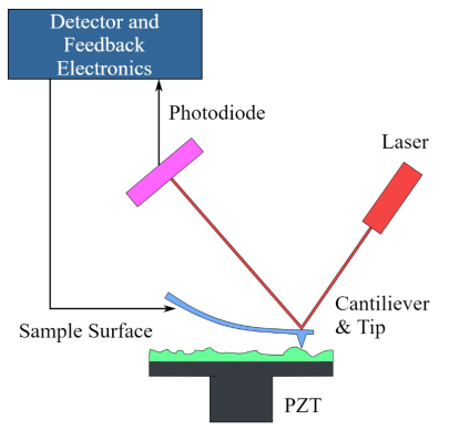
Fig. 1: Basic principle of AFM
Generally speaking, according to the contact condition between the probe and the sample surface during AFM operation, there are three working modes, as shown in Fig. 2 and Fig. 3: [3]
- Contact mode: during scanning, the probe is always in contact with the sample surface. Contact mode can achieve very fast scanning speeds and highly stable, high-resolution images; however, soft materials are easily deformed, and the probe wears out relatively easily.
- Non-contact mode: during scanning, the probe scans the sample at a height of 5–20 nm above the sample surface. In this working mode, the probe never contacts the surface, thus overcoming the damage and adsorption effects of the tip on the material surface in contact mode. However, due to the larger tip-sample distance, its resolution is lower than that of contact mode.
- Tapping mode: in this working mode, the probe continuously taps on the sample surface with a vibration amplitude of roughly tens to hundreds of nanometers. In tapping mode, the probe is always in instantaneous contact with the sample surface, eliminating the influence of lateral forces. Its resolution is close to that of contact mode, and it does not damage the sample surface. The disadvantage is a slower scanning speed.
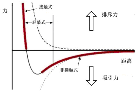
Fig. 2: Force-distance curve
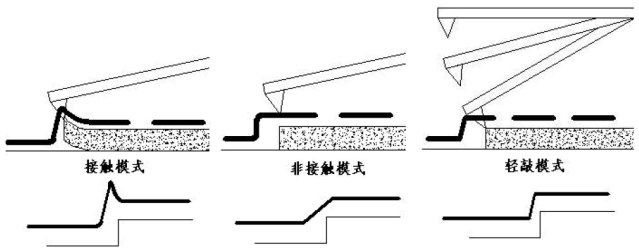
Fig. 3: The three working modes
Compared with other microscopy techniques, the most prominent advantage of AFM lies in its ability to image cells under near-physiological conditions. For example, in a saline environment, AFM achieves an imaging resolution of 30 nanometers for red blood cells. This feature provides scientists with a powerful tool for deeply investigating the structure of cell membranes and their membrane proteins while maintaining physiological conditions. AFM can perform molecular-level imaging of Langmuir-Blodgett (LB) films, clearly revealing individual polar head groups and the arrangement of molecules, even including their large-scale assembly structures. A major advantage of using LB films for research is that researchers can flexibly adjust the lipid composition in the film, thereby investigating lipid-lipid interactions, fluidity, and lipid-protein interactions. Research on LB films has found that AFM imaging results of biological samples are consistent with electron microscopy imaging in most cases, but the uniqueness of AFM lies in its ability to image under conditions closer to physiological environments, which electron microscopy cannot match.
In the field of physics, AFM is widely used to investigate the surface properties of metals and semiconductor materials, including surface morphology, reconstruction phenomena, surface electronic states, and dynamic processes. It can also reveal the surface structure of superconductors, electronic states, and charge density distributions in layered materials. Although theoretically the surface structure of metals can be predicted from their crystal structure, in reality the complexity of metal surfaces far exceeds imagination. Diffraction analysis techniques have revealed that in most cases, metal surfaces form superstructures (i.e., surface reconstruction) to minimize surface free energy. AFM technology demonstrates significant advantages in this regard, being able to conveniently capture reconstruction images of certain metals and semiconductor materials.
In the field of materials science, research on both inorganic and organic materials requires in-depth consultation of relevant literature to determine whether a material is crystalline or amorphous. Researchers also need to pay attention to the states of molecules or atoms, intermediate compounds, and various phase transitions, aiming to reveal the intrinsic relationship between material structure and properties. In this process, AFM allows researchers to directly observe, at the molecular or atomic microscopic level, the morphological features, defect structures, vacancy energies, aggregation energies, and various force interactions of crystals or amorphous materials. These direct observations play an extremely important role in deeply understanding and mastering the relationship between material structure and performance.
Thanks to AFM's broad applicability to samples and its microscopy performance, tapping-mode AFM is often combined with electrical and optical detection methods to form a new type of microscope — scattering-type scanning near-field optical microscopy (s-SNOM). s-SNOM is a precision imaging instrument that spans the working ranges of both optical microscopes and electron microscopes, with unique advantages: ultra-high resolution, non-destructive detection, real-time imaging, and the ability to obtain optical information from sample surfaces. [4] s-SNOM generally consists of an electrical/optical signal source, a detector, an AFM, and peripheral optics.
The principle of terahertz s-SNOM is shown in Fig. 4. Terahertz waves are focused onto the AFM probe, which operates in tapping mode vibrating at frequency Ω. The periodic vibration of the probe modulates the terahertz waves. After receiving the modulated terahertz waves, higher-harmonic demodulation is performed, which can effectively remove background signals and noise to obtain the near-field signal. By scanning point by point with the AFM probe, the near-field signal at each point of the sample is obtained, achieving near-field nano-imaging. The imaging resolution of s-SNOM depends only on the tip size of the probe, independent of the wavelength of the incident wave. This enables s-SNOM to break through the diffraction limit of traditional optical imaging and achieve nanoscale resolution comparable to AFM. [5]
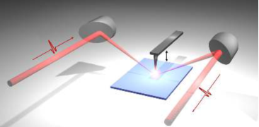
Fig. 4: Principle of terahertz s-SNOM
In 2022, Rainer Hillenbrand et al. demonstrated experimentally that despite complete background suppression, s-SNOM and nano-FTIR signals from material not located beneath the tip can be received through far-field reflection from the sample and scattering involving the tip. [6] Through detailed experimental and theoretical results, the authors showed that these artifacts can be identified and eliminated through a simple signal normalization step, thereby significantly enhancing the analytical capabilities of s-SNOM and nano-FTIR spectroscopy.
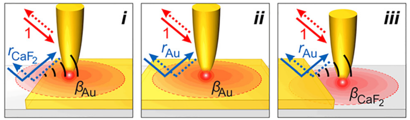
Fig. 5: Far-field reflection from the sample and scattering with the tip
As an example of far-field reflection artifacts, the authors performed s-SNOM imaging of an Au film on CaF2, as shown in Fig. 5. The experimental schematic is shown in Fig. 6: the incident field generated by a mid-infrared laser source is focused by a parabolic mirror (PM) onto an atomic force microscope tip in intermittent contact with the sample (tapping mode). The light scattered by the tip is collected by the same PM and recombined through a beam splitter (BS) with the beam from a movable reference mirror (RM) at the detector position. The experiment obtained the sample topography and optical signal sn images at orders 1 through 5, as shown in Fig. 7, where the optical amplitude is normalized to the center of the Au film.
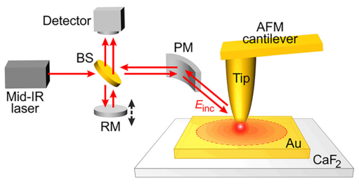
Fig. 6: Experimental schematic
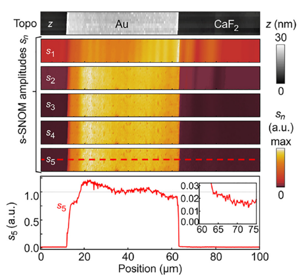
Fig. 7: Sample topography and optical signal images at various orders
Because the background noise was not suppressed, the outline of the gold film is almost invisible in the first-order signal amplitude map s1. At higher orders, the additive background is suppressed and the gold film outline is more easily identified. However, even at n = 5, the amplitude of s5 is not uniform (see the amplitude data plot of s5).
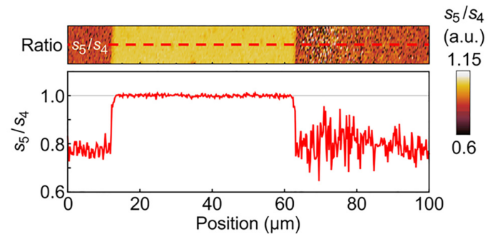
Fig. 8: Image and line profiles of the s5/s4 amplitude ratio
However, if two signals of different orders, such as s4 and s5, are used for normalization at this point, the background noise is greatly suppressed and the normalized amplitude becomes uniform. Fig. 8 shows the image and line profiles of the s5/s4 amplitude ratio.
The authors also show that the severity of these artifacts introduced by far-field reflection depends on the specific sample geometry. In many cases, these artifacts can be avoided or minimized. However, for complex sample geometries, the normalization method described above can eliminate the reflection artifacts.
References:
- Binnig G, Quate C F, Gerber Ch. Atomic Force Microscope[J]. Physical Review Letters, 1986, 56(9): 930-933.
- Atomic Force Microscope: Principle, Parts, Uses - Microbe Notes[EB]. (2023-06-05).
- Wang Xiang. Design of a tapping-mode atomic force microscope based on higher-order resonance[D]. Hefei University of Technology, 2011.
- Yue Dongdong, You Guanjun. Research on scattering-type terahertz scanning near-field optical microscopy[J]. Optical Instruments, 2020, 42(2): 64-69.
- Zhang Zhuocheng, Wang Yueying, Zhang Xiaoqiuyan, et al. Investigation of tip-sample interaction and its influence in terahertz scattering-type scanning near-field optical microscopy[J]. Acta Physica Sinica, 2021, 70(24): 248703-248707.
- Mester L, Govyadinov A A, Hillenbrand R. High-fidelity nano-FTIR spectroscopy by on-pixel normalization of signal harmonics[J]. Nanophotonics, 2022, 11(2): 377-390.