Author: Bin Zechuan
Background
In the terahertz and mid-infrared bands, with the rapid development of semiconductor plasmonics, graphene plasmon polaritons have demonstrated exceptional light confinement capability, and achieve high controllability and low-loss characteristics through tuning of the carrier density. In recent years, circuits based on graphene plasmons have been widely proposed for the transmission and processing of classical and quantum information. These circuits rely on electrostatic gating and possess active control functions that are difficult to achieve with traditional metal plasmonic circuits. Although the fundamental properties of graphene plasmons have been extensively studied through optical techniques such as far-field spectroscopy and near-field scanning optical microscopy, these methods are mainly limited to measuring the absorption of local plasmon resonances or standing-wave phenomena, and are not yet sufficient for the direct operation and control of plasmonic circuits.
Therefore, there is an urgent need for technologies that can effectively generate and dynamically control plasmonic signals, and measure their amplitude and phase on-chip. Yoshioka et al. combined on-chip terahertz time-domain spectroscopy with graphene-embedded coplanar waveguides and top-gate structures, injecting electrical pulses through ohmic contacts. This solved the momentum mismatch problem inherent in optical excitation and achieved efficient conversion of electrical pulses into plasmonic wave packets with a conversion efficiency of 35%, laying a solid foundation for the design and realization of graphene plasmonic circuits.
On-chip terahertz time-domain spectroscopy setup
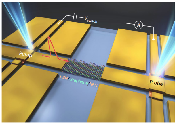
Fig. 1 Schematic of the device structure
This work adopts a structure design that integrates a graphene transistor into a coplanar waveguide (CPW), as shown in Fig. 1. Through ohmic contacts, terahertz electrical pulses are efficiently converted into graphene plasmon polaritons with a conversion efficiency of up to 35%. This technique enables researchers to directly generate and control plasmonic wave packets on graphene microstrips, successfully overcoming the momentum mismatch problem present in traditional optical excitation, thereby achieving picosecond-level spatiotemporal resolution of wave packet transmission.
Generation and propagation of graphene plasmons
This work designed different gate structures to generate and manipulate graphene plasmonic wave packets. Through electrical excitation, electrical pulses are converted into plasmonic wave packets with a duration of only 1.2 ps, and the three-dimensional confinement volume reaches 2.1 × 10⁻¹⁸ m³. This technique breaks through the limitations of traditional optical methods, achieving on-chip generation and manipulation of graphene plasmons.
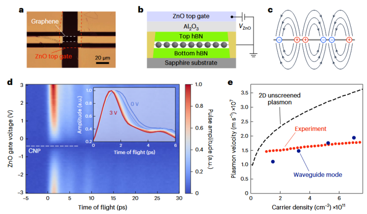
Fig. 2 Propagation of unscreened plasmons in the ZnO-gate device
This work first studied the propagation characteristics of unscreened graphene plasmonic wave packets in a zinc oxide gate device, as shown in Fig. 2a and 2b, where the graphene microstrip line is 8 μm wide and 23 μm long. Fig. 2d shows the time-domain waveform of the terahertz electrical pulse as a function of the zinc oxide gate voltage (VZnO = -3 to 3 V, carrier density n = -6.2 × 10¹¹ to 7.9 × 10¹¹ cm⁻²). The results in Fig. 2e show that by changing the zinc oxide gate voltage, the carrier density in the graphene can be adjusted, thereby affecting the propagation speed of the plasmons. As the carrier density increases, the plasmonic wave packets speed up and their pulse widths narrow. Furthermore, as shown in Fig. e, the experimentally measured wave packet velocities are close to the simulated values and are insensitive to carrier variations. The authors attribute this phenomenon to the formation of a waveguide mode in the graphene microstrip line, which was verified by varying the microstrip width.
Generation and propagation of acoustic graphene plasmons
In addition to the zinc oxide gate device, this work also studied the propagation characteristics of graphene plasmons in a gold top-gate device, as shown in Fig. 3a and 3b. Due to the screening effect of the Au gate, the propagation speed of acoustic plasmons is significantly reduced, exhibiting characteristics different from unscreened plasmons.
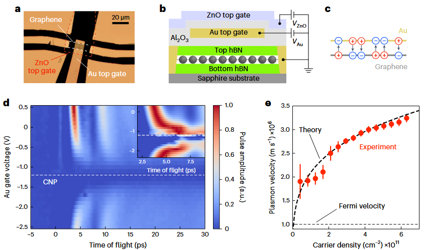
Fig. 3 Propagation of acoustic plasmons in the gold-gate device
Fig. 3 shows the propagation of acoustic plasmons. Under the screening effect of the Au gate, the propagation speed of acoustic plasmons drops to 1.9 × 10⁶ m/s, far lower than that of unscreened plasmons. In addition, by adjusting the gold gate voltage, this work precisely controlled the propagation speed and pulse width of the acoustic plasmonic wave packets. This indicates that the propagation of acoustic plasmons depends not only on the carrier density, but is also closely related to the screening effect between the graphene and the metal gate. Under high doping, the propagation distance of acoustic plasmons reached 21 μm.
Coherent and incoherent transport of ultrashort wave packets
As shown in Fig. 3e, when the carrier density n is less than 2 × 10¹¹ cm⁻², the measured velocity deviates from theoretical calculations. To analyze the cause of this phenomenon, this work analyzed the propagation characteristics of acoustic plasmons in the gold top-gate device based on an RLC distributed-constant circuit. As shown in Fig. 4a, due to the screening effect of the gold top gate, the propagation speed of acoustic plasmons is significantly lower than in the unscreened case and exhibits a linear dispersion relation. In addition, by adding a zinc oxide top gate between the gold top gate and the ohmic contact region to adjust the carrier density, this work optimized the impedance matching between the acoustic plasmons in graphene and the electrical pulses. In the highly doped region, the measured pulse duration is 1.2 ps, the propagation speed is 3.3 × 10⁶ m/s, and the wave packet is confined within a volume of 2.1 × 10⁻¹⁸ m³, demonstrating excellent spatial confinement characteristics.
As the carrier density decreases, the pulse width increases to 20 ps, indicating that near the charge neutrality point (CNP), the acoustic plasmons undergo a transition from coherent transport to incoherent diffusive transport. By solving the telegrapher's equations through simulation, this work successfully reproduced the experimental waveforms, as shown in Fig. 4a. This indicates that in highly doped regions, acoustic plasmons propagate coherently, while near the CNP, incoherent diffusive transport produces broader pulses.
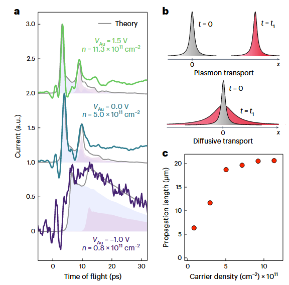
Fig. 4 Comparison of experimental and theoretical waveforms
Conversion efficiency of graphene plasmon polariton excitation
A major breakthrough of this study is the electrical excitation of graphene plasmonic wave packets, which significantly improves the conversion efficiency and overcomes certain limitations of optical excitation, such as momentum mismatch and the low nonlinear coefficient of graphene. This method achieves a conversion efficiency of up to 35% for unscreened plasmons and 3% for acoustic plasmons.
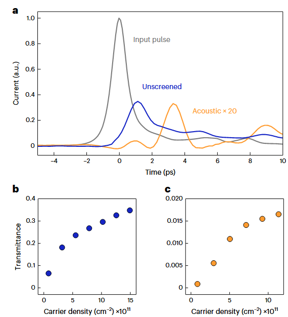
Fig. 5 Conversion efficiency of graphene plasmon polaritons
The experimental results show that in Fig. 5a, comparing the time-domain waveforms of the unscreened and acoustic plasmonic wave packets with the input electrical pulse, the transmittance (the ratio of the peak amplitudes of the output and input pulses) is mainly affected by three processes: the conversion of the input electrical pulse into a graphene plasmonic wave packet, the attenuation of the wave packet in graphene, and the conversion of the wave packet into an output electrical pulse. The transmittance provides a lower bound on the energy conversion efficiency, η = (Iplasmon/Iinput)². At high carrier densities, η for unscreened plasmons can exceed 0.35, while the maximum η for acoustic plasmons is 0.03 — both higher than the conversion efficiency of plasmons under optical excitation (η = 6 × 10⁻⁵). The key to this high conversion efficiency is that there is no energy loss due to momentum mismatch in the conversion between electrical pulses and plasmonic wave packets.
At this point, impedance mismatch becomes the main factor limiting device performance. In the gold top-gate device, the large difference between the electrical pulse velocity and the acoustic plasmon velocity leads to significant impedance mismatch. In the zinc oxide gate device, due to the higher plasmon velocity and the presence of transparent zinc oxide, the impedance mismatch is smaller, thereby improving the conversion efficiency.
Summary
Through terahertz electronics technology, this work successfully achieved on-chip generation, manipulation, and detection of ultrashort graphene plasmonic wave packets. This technological breakthrough not only overcomes the momentum mismatch problem in traditional optical excitation, but also makes significant progress in conversion efficiency and propagation characteristic research. In particular, unscreened plasmonic wave packets exhibit extremely high speed and coherence in zinc oxide gate devices, while acoustic plasmons demonstrate good propagation characteristics in gold gate devices. This terahertz electronics-based technology provides an efficient solution for the design of graphene plasmonic nanocircuits, not only improving the spatiotemporal resolution of the circuits, but also bringing new possibilities for future chip integration.
References
[1] YOSHIOKA K, BERNARD G, WAKAMURA T, et al. On-chip transfer of ultrashort graphene plasmon wave packets using terahertz electronics[J/OL]. Nature Electronics, 2024, 7(7): 537-544. DOI:10.1038/s41928-024-01197-x.