Author: Wang Ran
With the rapid development of photonics and nanotechnology, humanity's exploration of the microscopic world has entered a brand-new stage. Traditional optical microscopes, limited by the diffraction limit of light, struggle to achieve high-resolution imaging at subwavelength scales. However, scattering-type scanning near-field optical microscopy (s-SNOM), with its ability to surpass the diffraction limit, has become an important tool for studying the optical and chemical properties of nanomaterials. In this field, CO2 terahertz lasers, owing to their outstanding performance in the mid-infrared band, have been applied in many near-field studies. This article discusses near-field imaging technology based on CO2 terahertz lasers — particularly its applications in graphene and semiconductor nanodevices — drawing on several important works by the teams of Rainer Hillenbrand and Frank H. L. Koppens.
The CO2 terahertz laser is a laser widely used in the mid-infrared band. Its high energy and stability make it an ideal light source for near-field optical microscopy, and its pumping can generate high-intensity THz radiation with good monochromaticity, which can be further applied to near-field optics. s-SNOM uses a nanoscale probe to locally enhance the electromagnetic field, achieving super-resolution imaging at the nanoscale.
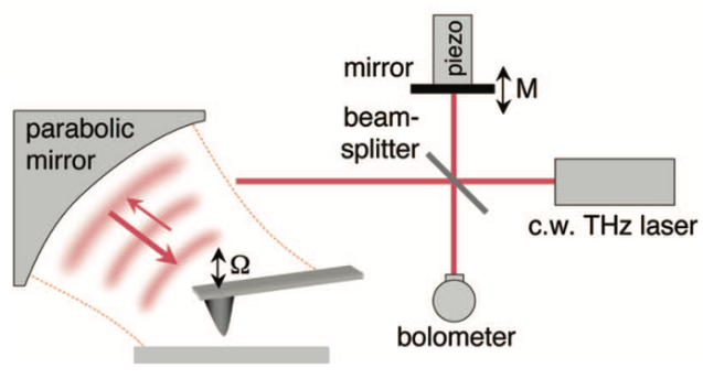
Fig. 1: Schematic of a THz s-SNOM setup based on CO2 laser pumping [1]
1. Light-matter interaction — graphene plasmons
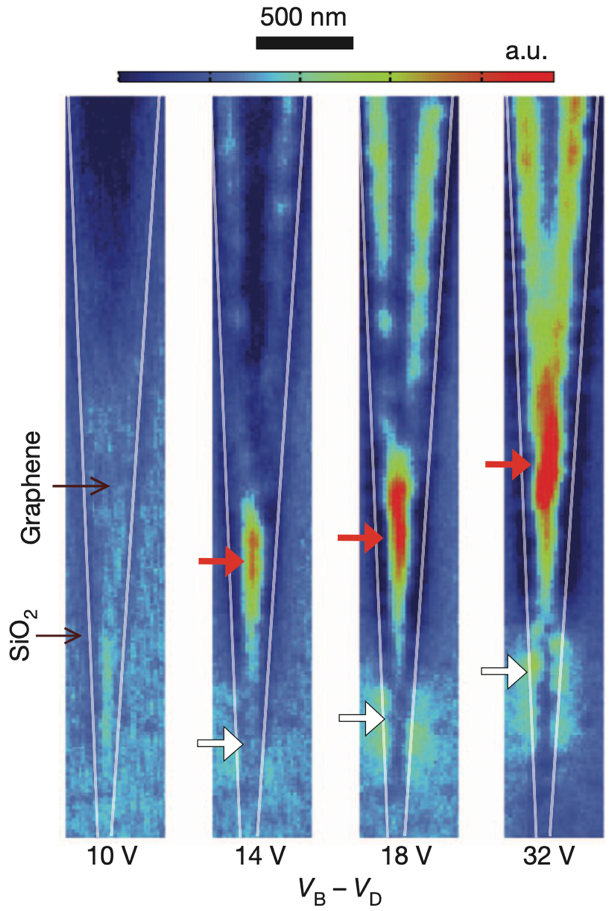
Hillenbrand and Koppens and their teams have done much pioneering work in this field, advancing the application of CO2 terahertz laser-based s-SNOM in nanomaterial research. Using a CO2 terahertz laser combined with near-field scanning optical microscopy, they successfully achieved imaging of plasmons in graphene [2]. By adjusting the Fermi level of graphene with an external gate voltage, they achieved dynamic control of the plasmons. This discovery is of great significance for developing graphene-based photonic devices, such as tunable optical transistors and nanoscale optical processing devices.
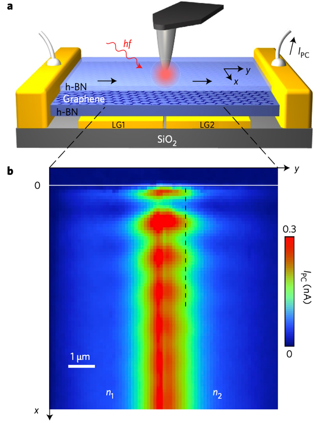
In addition to the near-field nano-imaging technology mentioned above, the two teams jointly proposed a near-field photocurrent nano-imaging technique, through which low-frequency (terahertz range) plasmons in graphene were observed experimentally for the first time [3]. These plasmons are closely related to the acoustic properties of graphene and are therefore called "acoustic plasmons". They are significantly influenced by electron-phonon interactions in graphene and can be regulated through external electric fields and the geometric structure of graphene, enabling precise control of their propagation behavior. This new near-field photocurrent microscopy technique will undoubtedly provide new perspectives for studying the complex optoelectronic
processes and physical properties in two-dimensional materials, and we look forward to more breakthroughs in this field in the future
Fig. 2 Plasmon gating of tapered graphene ribbons; local modes are indicated by white and red arrows, illumination wavelength. [2]
Fig. 3 THz photocurrent nano-imaging of dual-gated graphene plasmons. a. Schematic of the experimental setup. Laser illumination of the metal tip serves as a nanoscale near-field light source. The near-field-induced photocurrent in graphene (encapsulated by h-BN layers) is measured through the left and right metal contacts. LG1 and LG2 denote the dual gates (gold) on the left and right sides of the graphene, respectively, used to control the carrier concentration in the graphene. b. Experimental near-field photocurrent Ipc image recorded at f = 2.52 THz. Carrier densities n1 = 0.77 × 10¹² cm⁻², n2 = -0.71 × 10¹² cm⁻² were selected. The horizontal white solid line marks the edge of the graphene flake. [3]
2. Characterization of physical properties of semiconductor materials — strain and stress
In addition, the Hillenbrand team also used CO2 lasers for near-field imaging in the infrared band, successfully mapping strain field distributions in semiconductor materials at the nanoscale [4]. This non-destructive imaging technique demonstrates the advantages of CO2 lasers in detecting internal strain and stress distributions in semiconductor materials, which is of great significance for the design and optimization of semiconductor devices. Compared with other detection methods such as electron microscopy or X-ray diffraction, infrared near-field optical microscopy not only offers higher sensitivity, but can also image complex three-dimensional structures in a non-destructive manner, making it particularly suitable for studying the surface and subsurface properties of semiconductor materials.
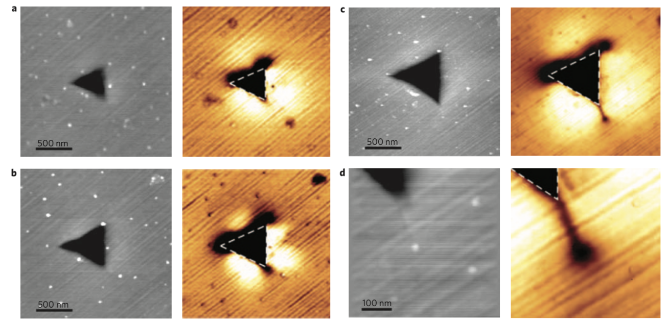
Fig. 4 s-SNOM images of nanoindentations in epitaxially grown SiC crystals. Loads of 7 mN (a), 10 mN (b), and 13 mN (c) were applied to a 30 μm thick crystal. The topography images (left) show that the size of the triangular indent increases with load, while the infrared images (right) reveal the spatial extent and asymmetry of the residual strain field. The systematic variation with applied load indicates that crack initiation is imminent at about 10 mN, identifiable by the reduced infrared signal directly at the lower corner of the indent. At a load of 13 mN, nanocracks form at the lower corner of the indent. d shows the residual strain field around the nanocrack and at the crack tip at higher resolution. [4]
3. Characterization of electrical properties of nanodevices — carrier concentration
In another study conducted by the Hillenbrand team, the researchers used the 2.54 THz band generated by a CO2 terahertz laser pumping CH3OH to probe the mobile carrier distribution in semiconductor nanodevices [1]. This study achieved a spatial resolution of about 40 nanometers through near-field microscopy, with extremely high sensitivity capable of detecting mobile carriers of fewer than 100 electrons, revealing the electrical properties of materials at the nanoscale.
The study also compared these results with imaging results obtained using the CO2 terahertz laser at 28 THz (mid-infrared). The terahertz signal revealed variations in carrier concentration within the transistor's silicon substrate in greater detail than the corresponding infrared near-field images. This comparative study demonstrates the complementarity of near-field imaging techniques in the THz and mid-infrared bands when probing the optical properties of materials. Particularly in semiconductor devices, the mid-infrared band of the CO2 terahertz laser can be used to probe the chemical composition and structure of materials, while the THz band is better suited for probing electrical properties such as carrier concentration and mobility.
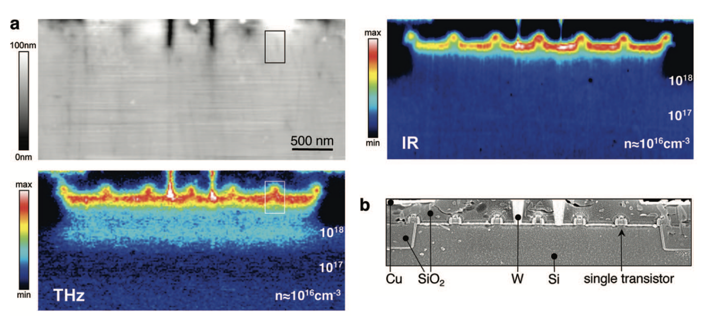
Fig. 5 Cross-sectional structure of a multi-transistor device under THz near-field microscopy. a. AFM topography (upper left) and simultaneously acquired terahertz near-field image (lower left); the varying terahertz signal within the silicon substrate reveals different mobile carrier concentrations. The infrared near-field image (upper right) clearly shows that variations in mobile carrier concentration can only be identified under terahertz illumination. b. SEM image of a similar but etched sample verifies that the terahertz image can distinguish different materials and individual transistors. [1]
In summary, the research conducted by Professor Rainer Hillenbrand, Professor Frank H. L. Koppens, and their teams using CO2 terahertz lasers in near-field optical microscopy demonstrates the powerful application potential of THz in multiple fields. These studies not only reveal the internal structures and dynamic behaviors of materials, but also provide new ideas for the design and development of future photonic devices. With further technological development, applications based on THz and infrared radiation will become more widespread — from ultra-high-sensitivity biosensors to novel quantum information processing devices, these technologies will play important roles in future scientific research and technological development.
Note: Main instruments used in the article
| Name | Model | Manufacturer |
| CO2 terahertz laser | SIFIR-50 | Coherent |
| Near-field AFM host | NeaSNOM | Nearspec |
| Detector | RSI-5T | Scontel |
Chengdu Miji Technology Co., Ltd. has long been committed to the development of near-field optical instrument technology, and can provide full-band near-field testing and product supply services covering visible, near-infrared, and terahertz ranges. Inquiries are welcome.
References
[1] Huber, A.J., et al., Terahertz Near-Field Nanoscopy of Mobile Carriers in Single Semiconductor Nanodevices. Nano Letters, 2008. 8(11): p. 3766-3770.
[2] Chen, J., et al. Optical nano-imaging of gate-tunable graphene plasmons. Nature, 2012. 487: 77–81.
[3] Alonso-González, P., et al. Acoustic terahertz graphene plasmons revealed by photocurrent nanoscopy. Nature Nanotechnology, 2017. 12: 31–35.
[4] Huber, A., et al. Infrared nanoscopy of strained semiconductors. Nature Nanotechnology, 2009. 4: 153–157.