Author: Bin Zechuan
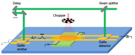
Background
Free-space terahertz time-domain spectroscopy has been widely applied to the study of various bulk materials and thin films. However, limited by the Rayleigh diffraction limit, terahertz beams are difficult to focus onto micrometer-sized samples, resulting in a significant reduction in the system's signal-to-noise ratio. Although terahertz near-field technology can break through the diffraction limit and achieve nanoscale resolution, the amplitude and bandwidth of its terahertz signal are still affected by water vapor absorption and optical path interference in free space [1]. To solve these problems, on-chip time-domain spectroscopy emerged. This technique confines terahertz pulses on a chip engraved with transmission lines, thereby circumventing the problems of the diffraction limit and water vapor absorption. Due to the high integration of the system, on-chip systems can be more conveniently combined with extreme conditions such as low temperature and strong magnetic fields compared with free-space systems.
At present, on-chip terahertz time-domain spectroscopy has been successfully applied to the study of electronic phases in carbon nanotubes at low temperature [2], topological insulators [3], and two-dimensional electron systems (such as GaAs and graphene) [4]. In addition, on-chip systems have been used to study two-dimensional van der Waals materials and their heterostructures, exploring key ultrafast processes triggered by their special interlayer coupling, such as interlayer hot-carrier dynamics, interlayer excitons, and shift currents. These studies demonstrate the great potential of on-chip terahertz time-domain spectroscopy in detecting and understanding complex electronic phenomena.
Working principle of the on-chip time-domain spectroscopy system
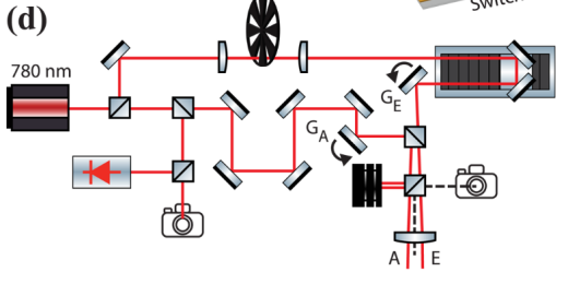
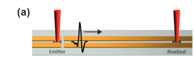
Fig. 1 (a) Optical path schematic of the on-chip time-domain spectroscopy system (b) On-chip transmission schematic
As shown in Fig. 1(a), a 3 mW, 780 nm, 75 fs, 250 MHz femtosecond laser is used to illuminate the photoconductive switches at the emitter and detector ends respectively. The excitation beam at the emitter end is modulated at a frequency of about 3.2 kHz, passes through an optical delay line, and is guided onto the emitter switch using a scanning galvanometer (GE). Meanwhile, a 10 V DC bias is applied to the emitter switch to provide the energy for conversion into THz transients. The generated terahertz pulses propagate along the coplanar stripline to the receiving end, where the excitation beam is guided and focused onto the switch through another scanning galvanometer (GA), thereby collecting the terahertz pulses at the receiving end and converting them into the corresponding photocurrent.
In practical applications, the signal bandwidth and dynamic range of on-chip time-domain spectroscopy systems are limited by the intrinsic properties of the photoconductive material — such as carrier lifetime, carrier mobility, dark current, and breakdown field — as well as the loss of the transmission line. Currently, semiconductor materials such as GaAs, LT-GaAs, InGaAs, and Er:GaAs [5] have been widely used in on-chip systems due to their short carrier lifetimes and high carrier mobilities. Meanwhile, to overcome transmission loss, different transmission structures are designed according to the actual research object, such as Goubau lines [6], coplanar striplines [1], and coplanar waveguides [7], to confine terahertz pulses between the waveguides as much as possible and achieve lower-loss terahertz transmission.
Ultrafast optoelectronic applications
With the exponential growth of data traffic, there is an urgent need for optical receivers with ultra-high bandwidth and low power consumption that can convert optical signals into electrical signals. Photothermoelectric effect (PTE) graphene photodetectors (PDs) are considered a powerful platform for photoelectric conversion due to their zero dark current operation, broadband absorption, and high conversion efficiency enabled by hot carrier multiplication (HCM). However, limited by the bandwidth of electronic readout equipment such as oscilloscopes and spectrum analyzers, experimental measurement bandwidth is restricted to below 70 GHz. Therefore, the carrier extraction mechanism remained unexplored. In 2022, Katsumasa Yoshioka et al. [8] used an on-chip ultrafast readout device (on-chip TDS) to successfully resolve the photoelectric conversion process in graphene, and found that photocurrent generation in graphene is quasi-instantaneous. The photocurrent at this point is mainly determined by the energy-level-dependent intraband scattering in graphene, independent of the carrier transit time, which is consistent with the Shockley-Ramo theorem — that is, in conductive materials such as graphene, photocurrent is generated immediately when ambient carriers enter the contacts. Compared with traditional optoelectronic readout methods, the photocurrent measured by the on-chip time-domain spectroscopy system directly tracks the development and evolution of carrier temperature, allowing researchers to resolve multiple coexisting thermalization and cooling pathways in graphene. The quantitative analysis of this photoelectric conversion process accelerates research into ultrafast graphene optoelectronic device engineering and lays a foundation for future optoelectronic device development.

Fig. 2: Schematic of the on-chip ultrafast electrical readout device and the measured time-domain and frequency-domain signals of the device.
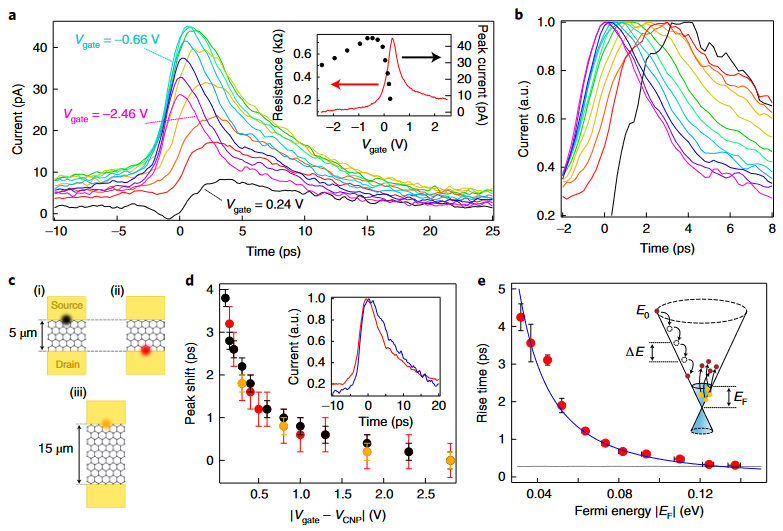
Fig. 3 Quasi-instantaneous photocurrent response
Hydrodynamic collective excitations in low-dimensional materials
Thermally excited electrons and holes form a quantum-critical Dirac fluid in ultra-clean graphene, whose electrodynamic response is described by a universal hydrodynamic theory. In this physical system, relativistic electrons and holes form a strongly interacting plasma. To date, the electrical transport signatures of the hydrodynamic Dirac fluid in graphene have been observed experimentally, including hydrodynamic electron flow [8], violation of the Wiedemann-Franz law [9], and quantum-critical conductivity [10]. However, the collective excitations of the hydrodynamic Dirac fluid, such as hydrodynamic bipolar plasmons and energy waves, remain at the prediction stage. Although these hydrodynamic collective excitations are well established in theory, their experimental observation in solid-state systems remains challenging. In 2023, Wenyu Zhao et al. [11] used on-chip time-domain spectroscopy to measure the THz absorption spectra of graphene microstrips and the propagation of energy waves in graphene near charge neutrality, successfully observing significant high-frequency hydrodynamic bipolar plasmon resonances and weaker low-frequency energy wave resonances. The results show that the hydrodynamic bipolar plasmon in graphene is an out-of-phase oscillation of massless electrons and holes, while the hydrodynamic energy wave is an electron-hole acoustic mode in which the two charge carriers oscillate in phase and move together. By changing the position of local thermal excitation in graphene, the researchers also successfully measured the propagation of energy waves at a characteristic velocity near charge neutrality. These studies provide new opportunities for exploring collective hydrodynamic excitations in low-dimensional materials.
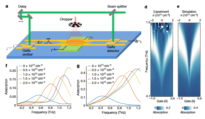
Fig. 4 Terahertz plasmons in graphene microstrips at 60 K (bipolar plasmon resonance)
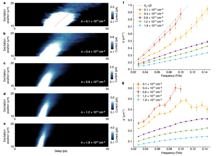
Fig. 5 Propagation of the Demon mode in graphene at 300 K (low-frequency energy wave resonance)
Cryogenic on-chip time-domain spectroscopy system
Typical THz pulses have an energy scale of a few meV and a time scale of picoseconds, making them ideal for studying strongly correlated phenomena, superconductivity, and non-equilibrium dynamics. However, due to the size limitations of free-space terahertz systems, many of these phenomena have not been fully explored at low temperatures. Thanks to its high integration, the on-chip time-domain spectroscopy system can be well combined with cryogenic systems. In 2023, Alex M. Potts et al. [12] proposed a cryogenic-compatible on-chip time-domain spectroscopy system with an interchangeable sample holder, which separates the test structure from the sample and greatly improves testing throughput. Using this system, the researchers measured the photoconductivity of niobium nitride (NbN) thin films only 7.5 micrometers wide, demonstrating the spectrometer's ability to detect the spectral signature of the superconducting gap in samples 2% smaller than the Rayleigh diffraction limit. The experimental results agree with the electromagnetic response in the superconducting state simulated by a disordered superconductor model, verifying the feasibility of the cryogenic on-chip time-domain spectroscopy system.

Fig. 6 Setup and optical path schematic of the cryogenic on-chip time-domain spectroscopy system
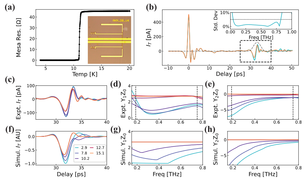
Fig. 7 On-chip terahertz spectra of superconducting NbN thin films
Summary
The on-chip time-domain spectroscopy system exploits the confinement of terahertz pulses by transmission lines to break through the Rayleigh diffraction limit, making it suitable for various small-area low-dimensional materials. This technique can shorten the pulse duration to the picosecond scale, which is crucial for studying and manipulating quantum materials, and will further accelerate progress in polariton research in van der Waals heterostructures and electron quantum optics research in quantum nanocircuits. In addition, the high integration of on-chip systems makes them easier to combine with cryogenic and strong magnetic field systems, thereby advancing ultrafast carrier dynamics research at millikelvin temperatures and in strong magnetic fields.
References
[1] Potts A M, Nayak A K, Nagel M, et al. On-chip time-domain terahertz spectroscopy of superconducting films below the diffraction limit[J]. Nano Letters, 2023, 23(9): 3835-3841.
[2] Zhong Z, Gabor N M, Sharping J E, et al. Terahertz time-domain measurement of ballistic electron resonance in a single-walled carbon nanotube[J]. Nature nanotechnology, 2008, 3(4): 201-205.
[3] Kastl C, Karnetzky C, Karl H, et al. Ultrafast helicity control of surface currents in topological insulators with near-unity fidelity[J]. Nature communications, 2015, 6(1): 6617.
[4] Wood C D, Mistry D, Li L H, et al. On-chip THz generation and detection at milli-Kelvin temperatures for the study of ultrafast phenomena in confined semiconductor systems[C]//2012 37th International Conference on Infrared, Millimeter, and Terahertz Waves. IEEE, 2012: 1-3.
[5] Potts A M. On-Chip Terahertz Time Domain Spectroscopy for Sub-Diffraction van der Waals Heterostructures[M]. University of California, Santa Barbara, 2023.
[6] Dazhang L, Cunningham J, Byrne M B, et al. On-chip terahertz Goubau-line waveguides with integrated photoconductive emitters and mode-discriminating detectors[J]. Applied Physics Letters, 2009, 95(9).
[7] Wood C D, Mistry D, Li L H, et al. On-chip terahertz spectroscopic techniques for measuring mesoscopic quantum systems[J]. Review of Scientific Instruments, 2013, 84(8).
[8] Ku M J H, Zhou T X, Li Q, et al. Imaging viscous flow of the Dirac fluid in graphene[J]. Nature, 2020, 583(7817): 537-541.
[9] Crossno J, Shi J K, Wang K, et al. Observation of the Dirac fluid and the breakdown of the Wiedemann-Franz law in graphene[J]. Science, 2016, 351(6277): 1058-1061.
[10] Gallagher P, Yang C S, Lyu T, et al. Quantum-critical conductivity of the Dirac fluid in graphene[J]. Science, 2019, 364(6436): 158-162.
[11] Zhao W, Wang S, Chen S, et al. Observation of hydrodynamic plasmons and energy waves in graphene[J]. Nature, 2023, 614(7949): 688-693.
[12] Potts A M, Nayak A K, Nagel M, et al. On-chip time-domain terahertz spectroscopy of superconducting films below the diffraction limit[J]. Nano Letters, 2023, 23(9): 3835-3841.