Author: Xu Xingxing
Terahertz scattering-type scanning near-field optical microscopy (THz s-SNOM) extends the application scenarios of terahertz technology to the micro- and nanoscale. It combines the advantages of terahertz technology and atomic force microscopy, bringing terahertz imaging resolution to a level comparable with atomic force microscopy — on the order of tens of nanometers — and has given rise to a series of important advances from research to applications.
This technology has developed rapidly in recent years, and its main application scenarios already cover multiple areas:
1. Testing the dielectric property distribution of materials
Just as terahertz far-field transmission/reflection experiments can yield the dielectric properties of a sample, terahertz near-field systems can also obtain dielectric properties — but within a very small region (tens of nanometers). In 2019, researchers from South Korea used a scattering-type scanning near-field microscope based on a terahertz time-domain spectrometer to test trace amounts of lactose in high-density polyethylene [1]. As shown in Fig. 1-1, the lactose region in the middle is only about 2 μm wide, and the curves on the right of Fig. 1-1 show that the lactose permittivity extracted from the near field is essentially consistent with that measured by conventional TDS. Taking advantage of this capability, in 2021 Professor Basov's group at Columbia University performed terahertz near-field imaging of WTe2 samples with different numbers of layers [2]. As shown in Fig. 1-2 (top), the imaging results indicate that monolayer to trilayer WTe2 exhibit weakly insulating, semiconducting, and metallic characteristics, respectively.
Since carrier concentration is also correlated with permittivity, terahertz near-field systems can also be used to test ion doping concentrations. Fig. 1-2 (bottom) shows near-field terahertz (2.54 THz) and infrared near-field imaging of a single transistor [3]. It can be seen that terahertz is more sensitive to carriers than infrared, indicating that terahertz near-field imaging systems have broad application prospects in the field of semiconductor inspection.
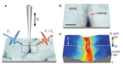
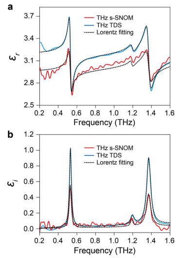
Fig. 1-1 Morphology and near-field imaging of the HDPE/lactose mixed sample (left), and comparison of the complex permittivity of lactose obtained from near-field/far-field measurements and Lorentz fitting
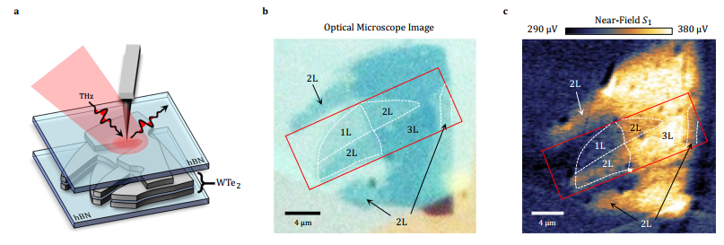

Fig. 1-2 Experimental schematic, optical imaging, and terahertz near-field imaging of WTe2 with different layer numbers (top); TEM imaging, infrared near-field imaging, terahertz near-field imaging of a single transistor, and the normalized terahertz signal along the white line (bottom)
2. Testing material plasmons
When a material has a resonant mode in the terahertz band, the carrier distribution on the material surface will be affected by that mode and exhibit a certain regularity. Since terahertz wavelengths are typically on the order of hundreds of micrometers, and the lifetime of material plasmons is very limited, observing this phenomenon in the terahertz band usually requires a relatively large confinement factor of the polariton. In 2017, the Rainer Hillenbrand group in Spain used a graphene-hBN-gold trilayer structure to achieve wavelength compression of graphene plasmons [4]. The confinement factor of this graphene acoustic plasmon reached 150 at 3.11 THz, allowing it to be observed by near-field photocurrent measurements. Six years later, the same group measured the surface plasmon distribution of the pure two-dimensional in-plane anisotropic material Ag2Te [5]. As shown in Fig. 2-2, the terahertz polariton confinement factor supported by this sample can reach 20 to 40; that observation used a terahertz scattering near-field imaging system based on a gas laser.
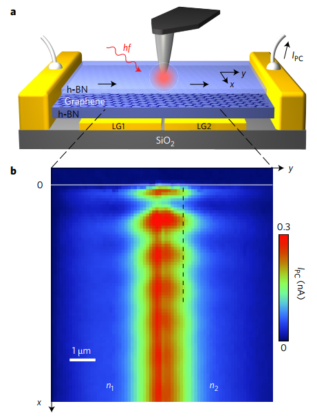
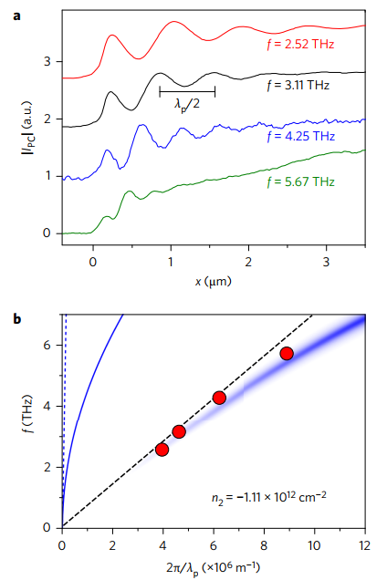
Fig. 2-1 Near-field photocurrent measurement of graphene acoustic plasmons
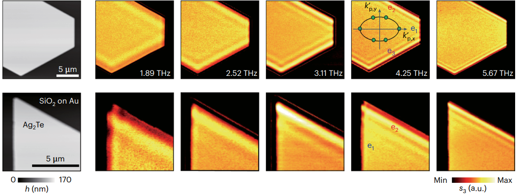
Fig. 2-2 Terahertz scattering near-field imaging results of two-dimensional Ag2Te material at different frequencies
3. Testing resonant field distributions of structures
Similar to plasmonic materials, metallic and dielectric structures can also support specific terahertz electromagnetic modes, thereby forming certain field distributions on their surfaces. The macroscopic manifestation in the far field is that after an electromagnetic wave passes through a metallic or dielectric structure, its amplitude, phase, polarization, and spectrum undergo specific changes. Using terahertz near-field systems, the electromagnetic mode distributions on metallic and dielectric surfaces can be observed more intuitively.
As shown in Fig. 3-1, a research team at the University of Leeds in the UK observed near-field imaging of a metallic antenna and a metallic split-ring resonator unit at 3.45 THz in 2021 [6], directly obtaining the surface electric field distributions of these two structures with a resolution of 35 nm. Fig. 3-2 also shows near-field imaging of a metallic split-ring resonator unit at 2.45 THz [7], but the authors found that the scattering direction of the probe for the near field is not constant, which causes the two adjacent boundaries at resonance to appear stronger than the background on one side and weaker than the background on the other in images at the resonant frequency.
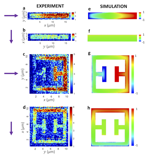
Fig. 3-1 Near-field imaging experiments and simulations of a metallic antenna and a metallic split-ring resonator unit at 3.45 THz; the arrow on the left indicates the polarization direction of the incident electric field
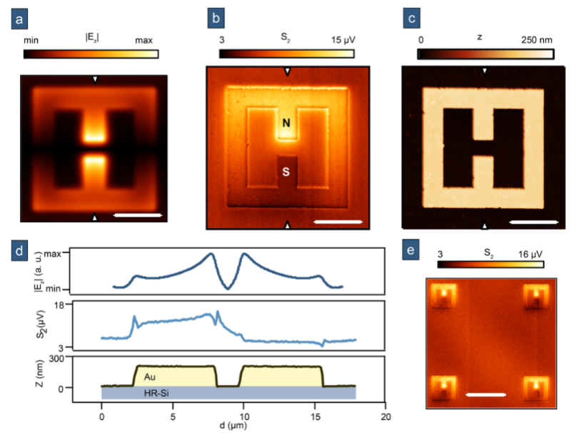
Fig. 3-2 a and b are the near-field simulation and experimental results of the split-ring structure at 2.45 THz, respectively; c is the AFM topography of the structure; d shows vertical line profiles at resonance, corresponding from top to bottom to a through c; e shows near-field imaging of multiple adjacent split rings, with a scale bar of 20 μm
Conclusion
Terahertz scattering near-field imaging systems have been developed for more than a decade. In addition to the research and application scenarios described above, frontier research such as near-field tomography and near-field ultrafast studies is also underway both at home and abroad, and more and more researchers are entering this field. Many important results are bound to emerge in the coming years, and we will continue to track and report on them. However, the international market for this system is mainly occupied by the German company Neaspec (acquired by attocube) and Bruker, while several domestic companies are also stepping up development. Chengdu Miji Technology Co., Ltd. was founded with the original aspiration of breaking the international monopoly on this system, and has now successfully developed a continuous-wave near-field imaging system below 1 THz, as well as a pulsed near-field imaging and spectroscopy system based on a terahertz time-domain spectrometer. Scholars and researchers from home and abroad are welcome to inquire.
References
[1] Moon K, Do Y, Park H, et al. Computed terahertz near-field mapping of molecular resonances of lactose stereo-isomer impurities with sub-attomole sensitivity[J]. Scientific Reports, 9.
[2] Jing R, Shao Y, Fei Z, et al. Terahertz response of monolayer and few-layer WTe 2 at the nanoscale[J]. Nature Communications, 2021.
[3] A. J. Huber, F. Keilmann, et al. Terahertz Near-Field Nanoscopy of Mobile Carriers in Single Semiconductor Nanodevices[J]. Nano Lett. 2008, 8, 11, 3766–3770.
[4] Alonso-González, P, Nikitin, A, Gao, Y. et al. Acoustic terahertz graphene plasmons revealed by photocurrent nanoscopy[J]. Nature Nanotech 12, 31–35 (2017).
[5] Chen, S, Leng, P. L, Konečná, A. et al. Real-space observation of ultraconfined in-plane anisotropic acoustic terahertz plasmon polaritons. Nat. Mater. 22, 860–866 (2023).
[6] Sulollari N , Keeley J, Park S J, et al. Coherent terahertz microscopy of modal field distributions in micro-resonators[J]. APL Photonics, 2021, 6(6).
[7] Thomas L, Théo. Hannotte, Santos C N, et al. Imaging of THz Photonic Modes by Scattering Scanning Near-Field Optical Microscopy[J]. ACS applied materials & interfaces, 2022, 14(28):32608-32617.