Author: Peng Bao
1. Research background and significance
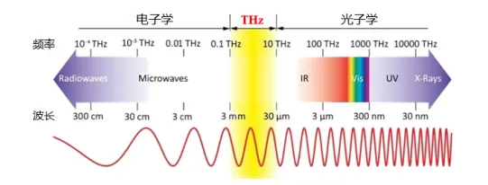
Terahertz waves (THz) generally refer to electromagnetic waves with frequencies in the range of 0.1 THz–10 THz (wavelengths of 3 mm–30 μm). In the electromagnetic spectrum, they lie between microwaves and infrared radiation, in the region transitioning from electronics to photonics, as shown by the yellow area in Fig. 1. It is precisely because of this special position that terahertz waves possess many advantages.
(1) Safety: low energy, non-damaging;
(2) Strong penetrability: good penetration through many non-polar and non-metallic materials;
(3) Fingerprint spectra: the THz band contains rich physical and chemical information, allowing analysis of the physicochemical properties of objects based on unique fingerprint spectral characteristics;
(4) Coherence: the amplitude and phase of the electric field can be measured, enabling extraction of the refractive index and absorption coefficient of samples;
(5) Transience: THz pulses typically last on the picosecond scale, providing high time-resolution capability.
In recent years, many scholars have applied terahertz wave imaging technology to disease diagnosis, but most work remains at the biological tissue level, and imaging research on cells is basically still a blank. Due to the long-wavelength nature of terahertz radiation (the wavelength of 1 THz is 300 μm), and affected by the diffraction limit, the detectable spatial resolution can hardly break through the half-wavelength size, failing to meet the imaging requirements for spatial resolution at the cellular and subcellular scales. Therefore, how to achieve terahertz imaging with higher spatial resolution has become a hot topic in the terahertz field.
Terahertz near-field imaging technology is expected to solve this problem, achieving micron- or even nanoscale spatial resolution. The term "near field" is relative to the "far field": the field distribution outside an object's surface can be divided into two parts by distance — the region within one wavelength of the object's surface is called the near-field region, and the region from one wavelength outward to infinity is called the far-field region. Traditional far-field imaging, limited by the diffraction limit, can hardly achieve an imaging spatial resolution beyond half the wavelength. The near field, by contrast, is studied within one wavelength of the sample surface, can break through the diffraction limit suffered by conventional optical microscopes, and its resolution is in principle not limited by the wavelength, thereby achieving higher imaging resolution.
2. Research status
Among the current methods for achieving high-resolution imaging using terahertz near-field technology, the common ones mainly include the confocal method, the aperture method, the tip-scattering method, and the transmission method. Today we mainly discuss the tip-scattering method and the transmission method.
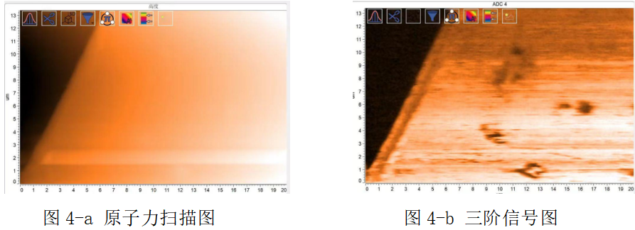
The basic principle of the tip-scattering method is to place a subwavelength micro-scatterer in the near-field region, using the micro-scatterer to scatter near-field signals into the far-field region. The terahertz detector can detect the induced terahertz waves associated with the tip's locally enhanced terahertz electric field region, as shown in Fig. 2. Its imaging spatial resolution depends on the radius of curvature of the tip, and can reach nanoscale spatial resolution. Our company has now successfully developed a terahertz nano near-field optical scanning system, as shown in Fig. 3, consisting of a terahertz time-domain spectrometer (TDS), an atomic force scanning microscope (AFM), and a lock-in amplifier. The TDS outputs terahertz waves, which are focused onto the atomic force probe through a free-space optical path via an off-axis mirror. Scanning the sample yields terahertz signals, including near-field signals, far-field signals, and background noise signals; after demodulation by the lock-in amplifier, a pure near-field signal is obtained, as shown in Fig. 4-b.
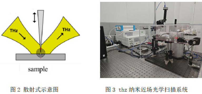
Actual test data (sample: contaminated gold sample, substrate: silicon)
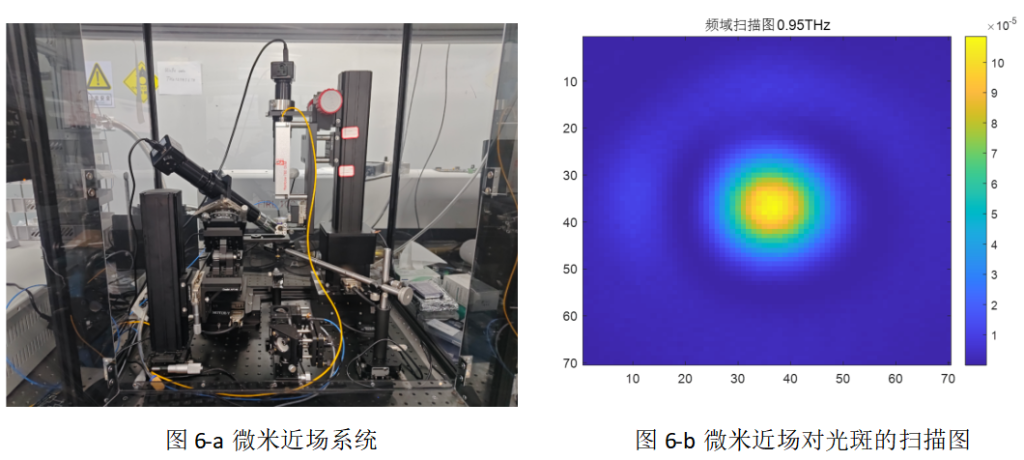
The transmission method, also known as the direct detection method, differs from the scattering-type terahertz scanning microscope, as shown in the schematic in Fig. 5. It achieves micron-level resolution, and its processing approach is also quite different. It works by minimizing the distance between the detector and the sample as much as possible and shrinking the detector size. Photoconductive probes are currently the most commonly used near-field detectors; they are essentially a pair of photoconductive antennas — miniature tapered antennas fabricated using a special lithography process, with an aperture size of only a few micrometers, which can eliminate the influence of stray light on the near-field signal. Our company has now successfully developed a micron near-field system with a resolution of 20 micrometers, offering a choice of probe scanning mode or sample scanning mode.
3. Final conclusion
Terahertz near-field optical systems can successfully break through the diffraction limit of traditional optics, pushing optical detection resolution to the micron and even nanoscale, with an applicable wavelength band covering visible to terahertz, achieving high-resolution, non-destructive, and quantitative detection from the physicochemical properties of materials to the structures of biological samples.
This technology demonstrates great application potential in fields such as polaritons in two-dimensional materials, semiconductor device characterization, and biological detection, providing a powerful tool for nanoscale scientific research. Our company is committed to research in terahertz-related fields and has launched multiple products. You are welcome to call us to inquire about related equipment.
References:
[1] Planken P C M, Valk N C J V D. Spot-size reduction in terahertz apertureless near-field imaging.[J]. Optics Letters, 2004, 29(19):2306-8.
[2] Chen HT, Kersting R, Cho GC. Terahertz imaging with nanometer resolution. Appl Phys Lett 2003, 83(15):3009-3011
[3] Knoll B, Keilmann F. Enhanced dielectric contrast in scattering-type scanning near-field optical
[4] microscopy. Opt Commun 2000, 182(4-6):321-328.
[5] Li Zaoxia. Development and application of a terahertz time-domain near-field system[D]. Changchun University of Science and Technology, 2019.
Chengdu Miji Technology Co., Ltd. has long been committed to the domestic production of high-end terahertz equipment and near-field optical equipment. The company will continue to follow international frontier developments in related fields and publish professional interpretations of relevant work — stay tuned. The company currently offers terahertz far-field imaging, spectroscopic time-domain systems, terahertz near-field imaging and spectroscopy systems, and terahertz photoconductive-probe near-field systems (micron-level resolution). Researchers interested in sample measurements are welcome to contact us and send samples for testing.